SNVS731B September 2011 – June 2019 LMR12010
PRODUCTION DATA.
- 1 Features
- 2 Applications
- 3 Description
- 4 Revision History
- 5 Pin Configuration and Functions
- 6 Specifications
- 7 Detailed Description
- 8 Application and Implementation
- 9 Layout
- 10Device and Documentation Support
- 11Mechanical, Packaging, and Orderable Information
Package Options
Refer to the PDF data sheet for device specific package drawings
Mechanical Data (Package|Pins)
- DDC|6
Thermal pad, mechanical data (Package|Pins)
Orderable Information
7.3.1 Boost Function
Capacitor CBOOST and diode D2 in Figure 15 are used to generate a voltage VBOOST. VBOOST – VSW is the gate-drive voltage to the internal NMOS control switch. To properly drive the internal NMOS switch during its on-time, VBOOST needs to be at least 1.6 V greater than VSW. Although the LMR12010 operates with this minimum voltage, it may not have sufficient gate drive to supply large values of output current. Therefore, it is recommended that VBOOST be greater than 2.5 V above VSW for best efficiency. VBOOST – VSW should not exceed the maximum operating limit of 5.5 V.
5.5 V > VBOOST – VSW > 2.5 V for best performance.
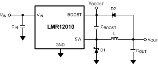 Figure 15. VOUT Charges CBOOST
 When the LMR12010 starts up, internal circuitry from the BOOST pin supplies a maximum of 20 mA to CBOOST. This current charges CBOOST to a voltage sufficient to turn the switch on. The BOOST pin continues to source current to CBOOST until the voltage at the feedback pin is greater than 0.76 V.
There are various methods to derive VBOOST:
- From the input voltage (VIN)
- From the output voltage (VOUT)
- From an external distributed voltage rail (VEXT)
- From a shunt or series zener diode
In the Functional Block Diagram, capacitor CBOOST and diode D2 supply the gate-drive current for the NMOS switch. Capacitor CBOOST is charged via diode D2 by VIN. During a normal switching cycle, when the internal NMOS control switch is off (TOFF) (refer to Figure 14), VBOOST equals VIN minus the forward voltage of D2 (VFD2), during which the current in the inductor (L) forward biases the Schottky diode D1 (VFD1). Therefore the voltage stored across CBOOST is
When the NMOS switch turns on (TON), the switch pin rises to
forcing VBOOST to rise thus reverse biasing D2. The voltage at VBOOST is then
which is approximately
for many applications. Thus the gate-drive voltage of the NMOS switch is approximately
An alternate method for charging CBOOST is to connect D2 to the output as shown in Figure 15. The output voltage must be between 2.5 V and 5.5 V, so that proper gate voltage will be applied to the internal switch. In this circuit, CBOOST provides a gate-drive voltage that is slightly less than VOUT.
In applications where both VIN and VOUT are greater than 5.5 V, or less than 3 V, CBOOST cannot be charged directly from these voltages. If VIN and VOUT are greater than 5.5 V, CBOOST can be charged from VIN or VOUT minus a zener voltage by placing a zener diode D3 in series with D2, as shown in Figure 16. When using a series zener diode from the input, ensure that the regulation of the input supply doesn’t create a voltage that falls outside the recommended VBOOST voltage.
(VINMAX – VD3) < 5.5 V
(VINMIN – VD3) > 1.6 V
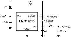 Figure 16. Zener Reduces Boost Voltage From VIN
 An alternative method is to place the zener diode D3 in a shunt configuration as shown in Figure 17. A small 350-mW to 500-mW, 5.1-V zener in a SOT-23 or SOD package can be used for this purpose. Place a small ceramic capacitor such as a 6.3-V, 0.1-µF capacitor (C4) in parallel with the zener diode. When the internal NMOS switch turns on, a pulse of current is drawn to charge the internal NMOS gate capacitance. The 0.1 µF parallel shunt capacitor ensures that the VBOOST voltage is maintained during this time.
Resistor R3 should be chosen to provide enough RMS current to the zener diode (D3) and to the BOOST pin. A recommended choice for the zener current (IZENER) is 1 mA. The current IBOOST into the BOOST pin supplies the gate current of the NMOS control switch and varies typically according to the following formula for the X version:
IBOOST can be calculated for the Y version using the following:
where
- D is the duty cycle
- VZENER and VD2 are in volts
- IBOOST is in milliamps
VZENER is the voltage applied to the anode of the boost diode (D2), and VD2 is the average forward voltage across D2. Note that this formula for IBOOST gives typical current. For the worst case IBOOST, increase the current by 40%. In that case, the worst case boost current will be
R3 will then be given by
For example, using the X-version let VIN = 10 V, VZENER = 5 V, VD2 = 0.7 V, IZENER = 1 mA, and duty cycle D = 50%. Then
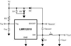 Figure 17. Boost Voltage Supplied From the Shunt Zener on VIN
 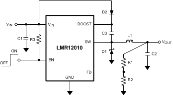 Figure 18. VBOOST Derived From VIN
 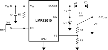 Figure 19. VBOOST Derived From Series Zener Diode (VOUT)