SLUSD87A March   2018  – January 2024 LMR14010A

PRODUCTION DATA  

  1.   1
  2. Features
  3. Applications
  4. Description
  5. Pin Configuration and Functions
  6. Specifications
    1. 5.1 Absolute Maximum Ratings
    2. 5.2 ESD Ratings
    3. 5.3 Recommended Operating Conditions
    4. 5.4 Thermal Information
    5. 5.5 Electrical Characteristics
    6. 5.6 Typical Characteristics
  7. Detailed Description
    1. 6.1 Overview
    2. 6.2 Functional Block Diagram
    3. 6.3 Feature Description
      1. 6.3.1 Fixed Frequency PWM Control
      2. 6.3.2 Bootstrap Voltage (CB)
      3. 6.3.3 Setting the Output Voltage
      4. 6.3.4 Enable ( SHDN ) and VIN Undervoltage Lockout
      5. 6.3.5 Current Limit
      6. 6.3.6 Thermal Shutdown
    4. 6.4 Device Functional Modes
      1. 6.4.1 Continuous Conduction Mode
      2. 6.4.2 Eco-mode
  8. Application and Implementation
    1. 7.1 Application Information
    2. 7.2 Typical Application
      1. 7.2.1 Design Requirements
        1. 7.2.1.1 Step-By-Step Design Procedure
      2. 7.2.2 Detailed Design Procedure
        1. 7.2.2.1 Custom Design With WEBENCH® Tools
        2. 7.2.2.2 Output Inductor Selection
        3. 7.2.2.3 Output Capacitor Selection
        4. 7.2.2.4 Schottky Diode Selection
        5. 7.2.2.5 Input Capacitor Selection
        6. 7.2.2.6 Bootstrap Capacitor Selection
      3. 7.2.3 Application Performance Curves
    3. 7.3 Power Supply Recommendations
    4. 7.4 Layout
      1. 7.4.1 Layout Guidelines
      2. 7.4.2 Layout Example
  9. Device and Documentation Support
    1. 8.1 Device Support
      1. 8.1.1 Development Support
        1. 8.1.1.1 Custom Design With WEBENCH® Tools
    2. 8.2 Receiving Notification of Documentation Updates
    3. 8.3 Support Resources
    4. 8.4 Trademarks
    5. 8.5 Electrostatic Discharge Caution
    6. 8.6 Glossary
  10. Revision History
  11. 10Mechanical, Packaging, and Orderable Information

Package Options

Mechanical Data (Package|Pins)
Thermal pad, mechanical data (Package|Pins)
Orderable Information

Pin Configuration and Functions

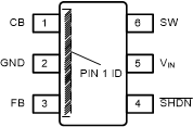
GUID-728531B2-8C93-4012-968E-6DA6C762C7B5-low.gifFigure 4-1 DDC Package, 6-Pin SOT-23-THIN (Top View)
Table 4-1 Pin Functions
PIN TYPE DESCRIPTION
NAME NO.
CB 1 I SW FET gate bias voltage. Connect Cboot capacitor between CB and SW.
FB 3 I Feedback Pin. Set feedback voltage divider ratio with VOUT = VFB (1+(R1/R2)).
GND 2 G Ground connection.
SHDN 4 I Enable and disable input pin(high voltage tolerant). Internal pull-up current source. Pull below 1.25 V to disable. Float to enable. Adjust the input undervoltage lockout with two resistors.
SW 6 O Switch node. Connect to inductor, diode and Cboot capacitor.
VIN 5 I Power input voltage pin. Input for internal supply and drain node input for internal high-side MOSFET.