SNVSAR4A December 2016 – April 2017 LMR23610-Q1
PRODUCTION DATA.
- 1 Features
- 2 Applications
- 3 Description
- 4 Revision History
- 5 Pin Configuration and Functions
- 6 Specifications
-
7 Detailed Description
- 7.1 Overview
- 7.2 Functional Block Diagram
- 7.3
Feature Description
- 7.3.1 Fixed Frequency Peak Current Mode Control
- 7.3.2 Adjustable Output Voltage
- 7.3.3 Enable/Sync
- 7.3.4 VCC, UVLO
- 7.3.5 Minimum ON-time, Minimum OFF-time and Frequency Foldback at Drop-out Conditions
- 7.3.6 Internal Compensation and CFF
- 7.3.7 Bootstrap Voltage (BOOT)
- 7.3.8 Over Current and Short Circuit Protection
- 7.3.9 Thermal Shutdown
- 7.4 Device Functional Modes
-
8 Application and Implementation
- 8.1 Application Information
- 8.2
Typical Applications
- 8.2.1 Design Requirements
- 8.2.2
Detailed Design Procedure
- 8.2.2.1 Custom Design With WEBENCH® Tools
- 8.2.2.2 Output Voltage Set-Point
- 8.2.2.3 Switching Frequency
- 8.2.2.4 Inductor Selection
- 8.2.2.5 Output Capacitor Selection
- 8.2.2.6 Feed-Forward Capacitor
- 8.2.2.7 Input Capacitor Selection
- 8.2.2.8 Bootstrap Capacitor Selection
- 8.2.2.9 VCC Capacitor Selection
- 8.2.2.10 Under Voltage Lockout Set-Point
- 8.2.3 Application Curves
- 9 Power Supply Recommendations
- 10Layout
- 11Device and Documentation Support
- 12Mechanical, Packaging, and Orderable Information
Package Options
Refer to the PDF data sheet for device specific package drawings
Mechanical Data (Package|Pins)
- DDA|8
Thermal pad, mechanical data (Package|Pins)
- DDA|8
Orderable Information
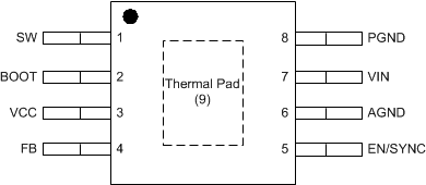
5 Pin Configuration and Functions
DDA Package
8-Pin HSOIC
Top View

Pin Functions
| PIN | I/O (1) | DESCRIPTION | |
|---|---|---|---|
| NAME | NO. | ||
| SW | 1 | P | Switching output of the regulator. Internally connected to both power MOSFETs. Connect to power inductor. |
| BOOT | 2 | P | Boot-strap capacitor connection for high-side driver. Connect a high quality 100 nF capacitor from BOOT to SW. |
| VCC | 3 | P | Internal bias supply output for bypassing. Connect a 2.2 μF/ 16 V or higher capacitance bypass capacitor from this pin to AGND. Do not connect external loading to this pin. Never short this pin to ground during operation. |
| FB | 4 | A | Feedback input to regulator, connect the feedback resistor divider tap to this pin. |
| EN/SYNC | 5 | A | Enable input to regulator. High = On, Low = Off. Can be connected to VIN. Do not float. Adjust the input under voltage lockout with two resistors. The internal oscillator can be synchronized to an external clock by coupling a positive pulse into this pin through a small coupling capacitor. See Enable/Sync for detail. |
| AGND | 6 | G | Analog ground pin. Ground reference for internal references and logic. Connect to system ground. |
| VIN | 7 | P | Input supply voltage. |
| PGND | 8 | G | Power ground pin, connected internally to the low side power FET. Connect to system ground, PAD, AGND, ground pins of CIN and COUT. Path to CIN must be as short as possible. |
| PAD | 9 | G | Low impedance connection to AGND. Connect to PGND on PCB. Major heat dissipation path of the die. Must be used for heat sinking to ground plane on PCB. |
(1) A = Analog, P = Power, G = Ground