SNVSB26C June 2018 – October 2020 LMR33630-Q1
PRODUCTION DATA
- 1 Features
- 2 Applications
- 3 Description
- 4 Revision History
- 5 Pin Configuration and Functions
- 6 Specifications
- 7 Detailed Description
-
8 Application and Implementation
- 8.1 Application Information
- 8.2
Typical Application
- 8.2.1 Design Requirements
- 8.2.2
Detailed Design Procedure
- 8.2.2.1 Custom Design With WEBENCH® Tools
- 8.2.2.2 Choosing the Switching Frequency
- 8.2.2.3 Setting the Output Voltage
- 8.2.2.4 Inductor Selection
- 8.2.2.5 Output Capacitor Selection
- 8.2.2.6 Input Capacitor Selection
- 8.2.2.7 CBOOT
- 8.2.2.8 VCC
- 8.2.2.9 CFF Selection
- 8.2.2.10 External UVLO
- 8.2.2.11 Maximum Ambient Temperature
- 8.2.3 Application Curves
- 8.3 What to Do and What Not to Do
- 9 Power Supply Recommendations
- 10Layout
- 11Device and Documentation Support
Package Options
Refer to the PDF data sheet for device specific package drawings
Mechanical Data (Package|Pins)
- RNX|12
Thermal pad, mechanical data (Package|Pins)
- RNX|12
Orderable Information
8.2.2.5 Output Capacitor Selection
The value of the output capacitor and the ESR of the capacitor determine the output voltage ripple and load transient performance. The output capacitor bank is usually limited by the load transient requirements, rather than the output voltage ripple. Equation 6 can be used to estimate a lower bound on the total output capacitance and an upper bound on the ESR, which is required to meet a specified load transient.
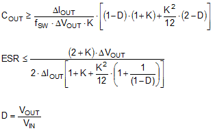
where
- ΔVOUT = output voltage transient
- ΔIOUT = output current transient
- K = ripple factor from Section 8.2.2.4
Once the output capacitor and ESR have been calculated, Equation 7 can be used to check the peak-to-peak output voltage ripple; Vr.
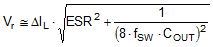
The output capacitor and ESR can then be adjusted to meet both the load transient and output ripple requirements.
For this example, a ΔVOUT ≤ 250 mV for an output current step of ΔIOUT = 2 A is required. Equation 6 gives a minimum value of 52 µF and a maximum ESR of 0.11 Ω. Assuming a 20% tolerance and a 10% bias de-rating, you arrive at a minimum capacitance of 72 µF. This can be achieved with a bank of 4 × 22-µF, 16-V ceramic capacitors in the 1210 case size. More output capacitance can be used to improve the load transient response. Ceramic capacitors can easily meet the minimum ESR requirements. In some cases, an aluminum electrolytic capacitor can be placed in parallel with the ceramics to help build up the required value of capacitance. In general, use a capacitor of at least 10 V for output voltages of 3.3 V or less and a capacitor of 16 V or more for output voltages of 5 V and above.
In practice, the output capacitor has the most influence on the transient response and loop phase margin. Load transient testing and Bode plots are the best way to validate any given design and must always be completed before the application goes into production. In addition to the required output capacitance, a small ceramic placed on the output can help reduce high frequency noise. Small case size ceramic capacitors in the range of 1 nF to 100 nF can be very helpful in reducing voltage spikes on the output caused by inductor and board parasitics.
The maximum value of total output capacitance must be limited to about 10 times the design value, or 1000 µF, whichever is smaller. Large values of output capacitance can adversely affect the start-up behavior of the regulator as well as the loop stability. If values larger than noted here must be used, then a careful study of start-up at full load and loop stability must be performed.