SNVSBA9B May 2019 – November 2020 LMR34215-Q1
PRODUCTION DATA
- 1 Features
- 2 Applications
- 3 Description
- 4 Revision History
- 5 Device Comparison Table
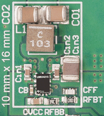
- 6 Pin Configuration and Functions
- 7 Specifications
- 8 Detailed Description
- 9 Power Supply Recommendations
- 10Layout
- 11Device and Documentation Support
- 12Mechanical, Packaging, and Orderable Information
Package Options
Mechanical Data (Package|Pins)
- RNX|12
Thermal pad, mechanical data (Package|Pins)
- RNX|12
Orderable Information
3 Description
The LMR34215-Q1 regulator is an easy-to-use, synchronous, step-down DC/DC converter. With integrated high-side and low-side power MOSFETs, output current is delivered over a wide input voltage range of 4.2 V to 42 V.
The LMR34215-Q1 uses peak-current-mode control to provide optimal efficiency and output voltage accuracy. Precision enable gives flexibility by enabling a direct connection to the wide input voltage or precise control over device start-up and shutdown. The power-good flag, with built-in filtering and delay, offers a true indication of system status eliminating the requirement for an external supervisor.
| PART NUMBER | PACKAGE(1) | BODY SIZE (NOM) |
|---|---|---|
| LMR34215-Q1 | VQFN-HR (12) | 2.00 mm × 3.00 mm |
 Simplified Schematic