SLUSEF4A June 2022 – November 2022 LMR51430
PRODUCTION DATA
- 1 Features
- 2 Applications
- 3 Description
- 4 Revision History
- 5 Device Comparison Table
- 6 Pin Configuration and Functions
- 7 Specifications
- 8 Detailed Description
- 9 Application and Implementation
- 10Device and Documentation Support
- 11Mechanical, Packaging, and Orderable Information
Package Options
Mechanical Data (Package|Pins)
- DDC|6
Thermal pad, mechanical data (Package|Pins)
Orderable Information
9.2.2.5 Output Capacitor Selection
The device is designed to be used with a wide variety of LC filters. Minimize the output capacitance to keep cost and size down. The output capacitor or capacitors, COUT, must be chosen with care because it directly affects the steady state output voltage ripple, loop stability, and output voltage overshoot and undershoot during load current transient. The output voltage ripple is essentially composed of two parts. One part is caused by the inductor ripple current flowing through the Equivalent Series Resistance (ESR) of the output capacitors:

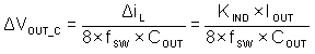
The other part is caused by the inductor current ripple charging and discharging the output capacitors:
The two components of the voltage ripple are not in-phase, therefore, the actual peak-to-peak ripple is less than the sum of the two peaks.
Output capacitance is usually limited by transient performance specifications if the system requires tight voltage regulation with presence of large current steps and fast slew rates. When a large load step occurs, output capacitors provide the required charge before the inductor current can slew to an appropriate level. The control loop of the converter usually requires eight or more clock cycles to regulate the inductor current equal to the new load level during this time. The output capacitance must be large enough to supply the current difference for eight clock cycles to maintain the output voltage within the specified range. Equation 14 shows the minimum output capacitance needed for a specified VOUT overshoot and undershoot.
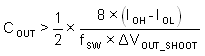
where
- KIND is the ripple ratio of the inductor current (ΔiL / IOUT).
- IOL is the low level output current during load transient.
- IOH is the high level output current during load transient.
- VOUT_SHOOT is the target output voltage overshoot or undershoot.
For this design example, the target output ripple is 30 mV. Assuming ΔVOUT_ESR = ΔVOUT_C = 30 mV, choose KIND = 0.3. Equation 12 yields ESR no larger than 75 mΩ and Equation 13 yields COUT no smaller than 14 µF. For the target overshoot and undershoot limitation of this design, ΔVOUT_SHOOT = 5% × VOUT = 250 mV. The COUT can be calculated to be no less than 48 µF by Equation 14. In summary, the most stringent criterion for the output capacitor is 48 µF. For this design, two 22-µF, 25-V, X7R ceramic capacitors with 5-mΩ ESR are used.