SNIS168E March 2013 – October 2017 LMT85
PRODUCTION DATA.
- 1 Features
- 2 Applications
- 3 Description
- 4 Revision History
- 5 Device Comparison Tables
- 6 Pin Configuration and Functions
- 7 Specifications
- 8 Detailed Description
- 9 Application and Implementation
- 10Power Supply Recommendations
- 11Layout
- 12Device and Documentation Support
- 13Mechanical, Packaging, and Orderable Information
Package Options
Mechanical Data (Package|Pins)
Thermal pad, mechanical data (Package|Pins)
Orderable Information
9 Application and Implementation
NOTE
Information in the following applications sections is not part of the TI component specification, and TI does not warrant its accuracy or completeness. TI’s customers are responsible for determining suitability of components for their purposes. Customers should validate and test their design implementation to confirm system functionality.
9.1 Application Information
The LMT85 features make it suitable for many general temperature-sensing applications. It can operate down to 1.8-V supply with 5.4-µA power consumption, making it ideal for battery powered devices. Package options like the through-hole TO-92 package allow the LMT85 to be mounted onboard, off-board, to a heat sink, or on multiple unique locations in the same application.
9.2 Typical Applications
9.2.1 Connection to an ADC
 Figure 13. Suggested Connection to a Sampling Analog-to-Digital Converter Input Stage
9.2.1.1 Design Requirements
Most CMOS ADCs found in microcontrollers and ASICs have a sampled data comparator input structure. When the ADC charges the sampling cap, it requires instantaneous charge from the output of the analog source such as the LMT85 temperature sensor and many op amps. This requirement is easily accommodated by the addition of a capacitor (CFILTER).
9.2.1.2 Detailed Design Procedure
The size of CFILTER depends on the size of the sampling capacitor and the sampling frequency. Because not all ADCs have identical input stages, the charge requirements will vary. This general ADC application is shown as an example only.
9.2.1.3 Application Curve
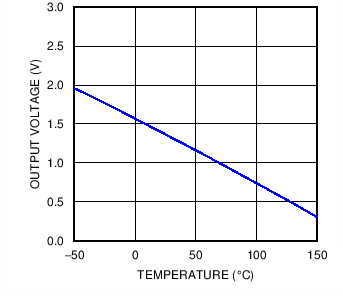 Figure 14. Analog Output Transfer Function
9.2.2 Conserving Power Dissipation With Shutdown
 Figure 15. Simple Shutdown Connection of the LMT85
9.2.2.1 Design Requirements
Because the power consumption of the LMT85 is less than 9 µA, it can simply be powered directly from any logic gate output and therefore not require a specific shutdown pin. The device can even be powered directly from a micro controller GPIO. In this way, it can easily be turned off for cases such as battery-powered systems where power savings are critical.
9.2.2.2 Detailed Design Procedure
Simply connect the VDD pin of the LMT85 directly to the logic shutdown signal from a microcontroller.
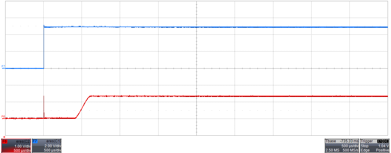
9.2.2.3 Application Curves
INDENT:
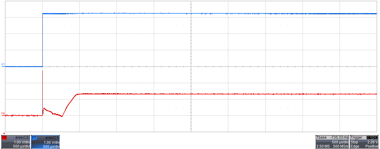
Time: 500 µs/div; Top Trace: VDD 1 V/div;Bottom Trace: OUT 1 V/div
INDENT:
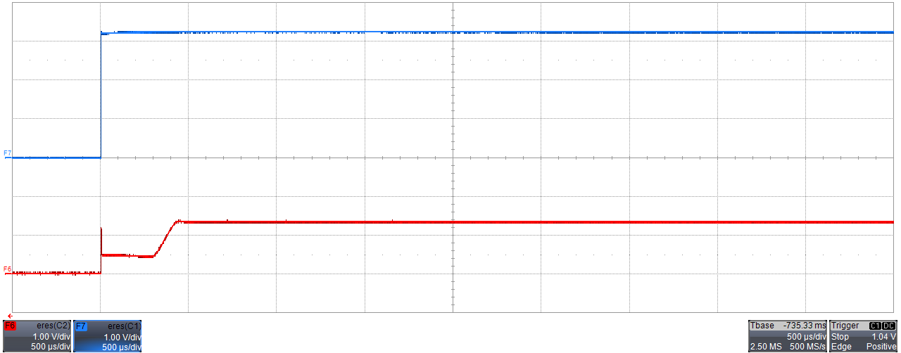
Time: 500 µs/div; Top trace: VDD 1V/div;Bottom trace: OUT 1 V/div
INDENT:
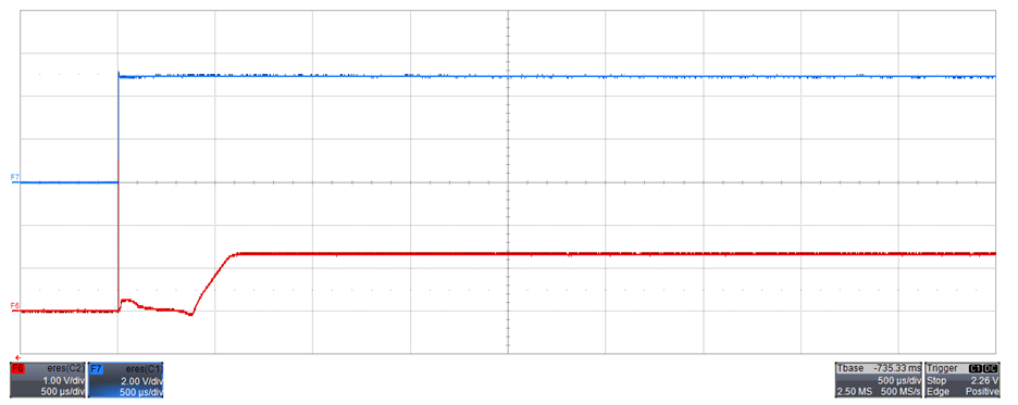
Time: 500 µs/div; Top trace: VDD 2 V/div;Bottom trace: OUT 1 V/div
INDENT:
Time: 500 µs/div; Top trace: VDD 2 V/div;Bottom trace: OUT 1 V/div