SNIS202A October   2017  – June 2022 LMT87-Q1

PRODUCTION DATA  

  1. Features
  2. Applications
  3. Description
  4. Revision History
  5. Device Comparison
  6. Pin Configuration and Functions
  7. Specifications
    1. 7.1 Absolute Maximum Ratings
    2. 7.2 ESD Ratings
    3. 7.3 Recommended Operating Conditions
    4. 7.4 Thermal Information
    5. 7.5 Accuracy Characteristics
    6. 7.6 Electrical Characteristics
    7. 7.7 Typical Characteristics
  8. Detailed Description
    1. 8.1 Overview
    2. 8.2 Functional Block Diagram
    3. 8.3 Feature Description
      1. 8.3.1 LMT87-Q1 Transfer Function
    4. 8.4 Device Functional Modes
      1. 8.4.1 Mounting and Thermal Conductivity
      2. 8.4.2 Output Noise Considerations
      3. 8.4.3 Capacitive Loads
      4. 8.4.4 Output Voltage Shift
  9. Application and Implementation
    1. 9.1 Application Information
    2. 9.2 Typical Applications
      1. 9.2.1 Connection to ADC
        1. 9.2.1.1 Design Requirements
        2. 9.2.1.2 Detailed Design Procedure
        3. 9.2.1.3 Application Curve
      2. 9.2.2 Conserving Power Dissipation With Shutdown
        1. 9.2.2.1 Design Requirements
        2. 9.2.2.2 Detailed Design Procedure
        3. 9.2.2.3 Application Curves
  10. 10Power Supply Recommendations
  11. 11Layout
    1. 11.1 Layout Guidelines
    2. 11.2 Layout Example
  12. 12Device and Documentation Support
    1. 12.1 Receiving Notification of Documentation Updates
    2. 12.2 Support Resources
    3. 12.3 Trademarks
    4. 12.4 Electrostatic Discharge Caution
    5. 12.5 Glossary
  13. 13Mechanical, Packaging, and Orderable Information

Package Options

Mechanical Data (Package|Pins)
Thermal pad, mechanical data (Package|Pins)
Orderable Information

Pin Configuration and Functions

GUID-6F10859A-C833-4C61-8A03-A7B43F362F9B-low.gifFigure 6-1 DCK Package5-Pin SOT (SC70)Top View
Table 6-1 Pin Functions
PIN TYPE DESCRIPTION
NAME SOT (SC70) EQUIVALENT CIRCUIT FUNCTION
GND 2(1) Ground N/A Power Supply Ground
OUT 3 Analog
Output
GUID-233FA44A-7440-40D7-AE3B-6CED36AEBBFC-low.gif 
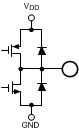
Outputs a voltage that is inversely proportional to temperature
VDD 1, 4, 5 Power N/A Positive Supply Voltage
Direct connection to the back side of the die