SNIS176A March 2013 – January 2015 LMT89
PRODUCTION DATA.
- 1 Features
- 2 Applications
- 3 Description
- 4 Revision History
- 5 Pin Configuration and Functions
- 6 Specifications
- 7 Detailed Description
- 8 Application and Implementation
- 9 Power Supply Recommendations
- 10Layout
- 11Device and Documentation Support
- 12Mechanical, Packaging, and Orderable Information
Package Options
Mechanical Data (Package|Pins)
- DCK|5
Thermal pad, mechanical data (Package|Pins)
Orderable Information
8 Application and Implementation
NOTE
Information in the following applications sections is not part of the TI component specification, and TI does not warrant its accuracy or completeness. TI’s customers are responsible for determining suitability of components for their purposes. Customers should validate and test their design implementation to confirm system functionality.
8.1 Application Information
The LMT89 has a very low supply current and a wide supply range therefore it can easily be driven by a battery as shown in Figure 4.
8.1.1 Capacitive Loads
The LMT89 device handles capacitive loading well. Without any precautions, the LMT89 device can drive any capacitive load less than 300 pF as shown in Figure 2. The specified temperature range the LMT89 device has a maximum output impedance of 160 Ω. In an extremely noisy environment it may be necessary to add some filtering to minimize noise pickup. TI recommends that 0.1 μF be added from V+ to GND to bypass the power supply voltage, as shown in Figure 2. In a noisy environment it may even be necessary to add a capacitor from the output to ground with a series resistor as shown in Figure 2. A 1-μF output capacitor with the 160-Ω maximum output impedance and a 200-Ω series resistor will form a 442-Hz lowpass filter. Because the thermal time constant of the LMT89 device is much slower, the overall response time of the LMT89 device will not be significantly affected.
In situations where a transient load current is placed on the circuit output, the series resistance value may be increased to compensate for any ringing that may be observed.
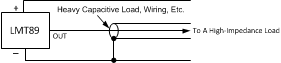 Figure 2. LMT89 No Decoupling Required for Capacitive Loads Less Than 300 pF
Table 2. Design Parameters
| Minimum R (Ω) | C (µF) |
|---|---|
| 200 | 1 |
| 470 | 0.1 |
| 680 | 0.01 |
| 1 k | 0.001 |
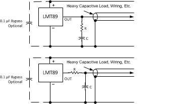 Figure 3. LMT89 With Filter for Noisy Environment and Capacitive Loading Greater Than 300 pF
NOTE
Either placement of resistor, as shown in and , is just as effective.
8.2 Typical Applications
8.2.1 Full-Range Centigrade Temperature Sensor
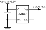 Figure 4. Full-Range Celsius (Centigrade) Temperature Sensor (−55°C to 130°C) Operating from a Single Li-Ion Battery Cell
8.2.1.1 Design Requirements
Design requirements related to layout are also important because the LMT89 device is a simple temperature sensor that provides an analog output, refer to Layout for a detailed description.
8.2.1.2 Detailed Design Procedure
The LMT89 device output is shown in Equation 4.
Solve for T as shown in Equation 5:
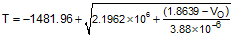
where
- T is temperature, and VO is the measured output voltage of the LMT89 device. Equation 5 is the most accurate equation that can be used to calculate the temperature of the LMT89 device.
An alternative to the quadratic equation a second order transfer function can be determined using the least squares method shown in Equation 6.
where
- T is temperature express in °C and VO is the output voltage expressed in volts.
A linear transfer function can be used over a limited temperature range by calculating a slope and offset that give best results over that range. A linear transfer function can be calculated from the parabolic transfer function of the LMT89 device. The slope of the linear transfer function can be calculated using Equation 7.
where
- T is the middle of the temperature range of interest and m is in V/°C. For example for the temperature range of TMIN = −30 to TMAX = 100°C
and
The offset of the linear transfer function can be calculated using Equation 10.
where
- VOP(TMAX) is the calculated output voltage at TMAX using the parabolic transfer function for VO.
- VOP(T) is the calculated output voltage at T using the parabolic transfer function for VO.
The best fit linear transfer function for many popular temperature ranges was calculated in Table 3. As shown in Table 3, the error introduced by the linear transfer function increases with wider temperature ranges.
Table 3. First Order Equations Optimized for Different Temperature Ranges
| TEMPERATURE RANGE | LINEAR EQUATION | MAXIMUM DEVIATION OF LINEAR EQUATION FROM PARABOLIC EQUATION (°C) |
|
|---|---|---|---|
| Tmin (°C) | Tmax (°C) | ||
| −55 | 130 | VO = −11.79 mV/°C × T + 1.8528 V | ±1.41 |
| −40 | 110 | VO = −11.77 mV/°C × T + 1.8577 V | ±0.93 |
| −30 | 100 | VO = −11.77 mV/°C × T + 1.8605 V | ±0.70 |
| -40 | 85 | VO = −11.67 mV/°C × T + 1.8583 V | ±0.65 |
| −10 | 65 | VO = −11.71 mV/°C × T + 1.8641 V | ±0.23 |
| 35 | 45 | VO = −11.81 mV/°C × T + 1.8701 V | ±0.004 |
| 20 | 30 | VO = –11.69 mV/°C × T + 1.8663 V | ±0.004 |
8.2.1.3 Application Curve
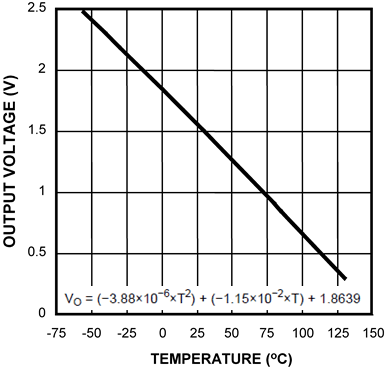 Figure 5. Output Voltage vs Temperature
8.2.2 Centigrade Thermostat
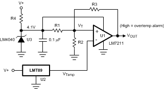 Figure 6. Centigrade Thermostat
8.2.2.1 Design Requirements
A simple thermostat can be created by using a reference (LM4040) and a comparator (LM7211) as shown in Figure 6.
8.2.2.2 Detailed Design Procedure
The threshold values can be calculated using Equation 11 and Equation 12.


8.2.2.3 Application Curve
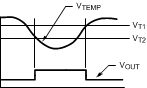 Figure 7. Thermostat Output Waveform
8.3 System Examples
8.3.1 Conserving Power Dissipation With Shutdown
The LMT89 device draws very little power therefore it can simply be shutdown by driving its supply pin with the output of an logic gate as shown in Figure 8.
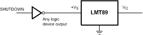 Figure 8. Conserving Power Dissipation With Shutdown
8.3.2 Analog-to-Digital Converter Input Stage
Most CMOS ADCs found in ASICs have a sampled data comparator input structure that is notorious for causing problems for analog output devices, such as the LMT89 and many op amps. The cause of this difficulty is the requirement of instantaneous charge of the input sampling capacitor in the ADC. This requirement is easily accommodated by the addition of a capacitor. Because not all ADCs have identical input stages, the charge requirements will vary necessitating a different value of compensating capacitor. This ADC is shown as an example only. If a digital output temperature is required, refer to devices such as the LM74 device.
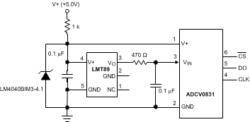 Figure 9. Suggested Connection to a Sampling Analog-to-Digital Converter Input Stage