SNOSA87C October 2003 – October 2016 LMV116 , LMV118
PRODUCTION DATA.
- 1 Features
- 2 Applications
- 3 Description
- 4 Revision History
- 5 Pin Configuration and Functions
- 6 Specifications
- 7 Detailed Description
- 8 Application and Implementation
- 9 Power Supply Recommendations
- 10Layout
- 11Device and Documentation Support
- 12Mechanical, Packaging, and Orderable Information
Package Options
Mechanical Data (Package|Pins)
- DBV|5
Thermal pad, mechanical data (Package|Pins)
Orderable Information
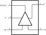
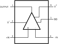
5 Pin Configuration and Functions
SOT-23 Package
5-Pin DBV
Top View

SOT-23 Package
6-Pin DBV
Top View

Pin Functions
| PIN | I/O | DESCRIPTION | ||
|---|---|---|---|---|
| NAME | LMV116 | LMV118 | ||
| +IN | 3 | 3 | Input | Non-inverting input |
| –IN | 4 | 4 | Input | Inverting input |
| OUTPUT | 1 | 1 | Output | Output |
| SD | — | 5 | Input | Shutdown input. Active high, must be tied to V– with resistor for normal operation. |
| V+ | 5 | 6 | Power | Positive (highest) power supply |
| V– | 2 | 2 | Power | Negative (lowest) power supply |