SNOS519K April   2000  – August 2016 LMV710-N

PRODUCTION DATA.  

  1. Features
  2. Applications
  3. Description
  4. Revision History
  5. Pin Configuration and Functions
  6. Specifications
    1. 6.1 Absolute Maximum Ratings
    2. 6.2 ESD Ratings
    3. 6.3 Recommended Operating Conditions
    4. 6.4 Thermal Information
    5. 6.5 Electrical Characteristics - 2.7 V
    6. 6.6 Electrical Characteristics - 3.2 V
    7. 6.7 Electrical Characteristics - 5 V
    8. 6.8 Typical Characteristics
  7. Detailed Description
    1. 7.1 Overview
    2. 7.2 Functional Block Diagram
    3. 7.3 Feature Description
      1. 7.3.1 Supply Bypassing
      2. 7.3.2 Shutdown Mode
      3. 7.3.3 Rail-to-Rail Input
    4. 7.4 Device Functional Modes
      1. 7.4.1 Compensation of Input Capacitance
      2. 7.4.2 Capacitive Load Tolerance
  8. Application and Implementation
    1. 8.1 Application Information
    2. 8.2 Typical Applications
      1. 8.2.1 High-Side Current-Sensing
        1. 8.2.1.1 Design Requirements
        2. 8.2.1.2 Detailed Design Procedure
        3. 8.2.1.3 Application Curve
      2. 8.2.2 Peak Detector
        1. 8.2.2.1 Design Requirements
        2. 8.2.2.2 Detailed Design Procedure
      3. 8.2.3 GSM Power Amplifier Control Loop
        1. 8.2.3.1 Design Requirements
        2. 8.2.3.2 Detailed Design Procedure
  9. Power Supply Recommendations
  10. 10Layout
    1. 10.1 Layout Guidelines
    2. 10.2 Layout Example
  11. 11Device and Documentation Support
    1. 11.1 Device Support
      1. 11.1.1 Development Support
    2. 11.2 Documentation Support
      1. 11.2.1 Related Documentation
    3. 11.3 Related Links
    4. 11.4 Receiving Notification of Documentation Updates
    5. 11.5 Community Resources
    6. 11.6 Trademarks
    7. 11.7 Electrostatic Discharge Caution
    8. 11.8 Glossary
  12. 12Mechanical, Packaging, and Orderable Information

Package Options

Mechanical Data (Package|Pins)
Thermal pad, mechanical data (Package|Pins)
Orderable Information

10 Layout

10.1 Layout Guidelines

To properly bypass the power supply, several locations on a printed-circuit board must be considered. A 6.8-µF or greater tantalum capacitor must be placed at the point where the power supply for the amplifier is introduced onto the board. Another 0.1-µF ceramic capacitor must be placed as close as possible to the power supply pin of the amplifier. If the amplifier is operated in a single power supply, only the V+ pin requires a bypass with a 0.1-µF capacitor. If the amplifier is operated in a dual power supply, both V+ and V pins must be bypassed. It is good practice to use a ground plane on a printed-circuit board to provide all components with a low inductive ground connection.

10.2 Layout Example
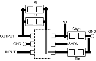
LMV710-N LMV711-N LMV715-N LMV711_LAYOUT.gif Figure 45. LMV711 Layout Example