SNOS032I August 1999 – June 2016 LMV821-N , LMV822-N , LMV822-N-Q1 , LMV824-N , LMV824-N-Q1
PRODUCTION DATA.
- 1 Features
- 2 Applications
- 3 Description
- 4 Revision History
- 5 Pin Configuration and Functions
-
6 Specifications
- 6.1 Absolute Maximum Ratings
- 6.2 ESD Ratings
- 6.3 Recommended Operating Conditions
- 6.4 Thermal Information, 5 Pins
- 6.5 Thermal Information, 8 Pins
- 6.6 Thermal Information, 14 Pins
- 6.7 DC Electrical Characteristics 2.7V
- 6.8 DC Electrical Characteristics 2.5V
- 6.9 AC Electrical Characteristics 2.7V
- 6.10 DC Electrical Characteristics 5V
- 6.11 AC Electrical Characteristics 5V
- 6.12 Typical Characteristics
- 7 Detailed Description
- 8 Application and Implementation
- 9 Power Supply Recommendations
- 10Layout
- 11Device and Documentation Support
- 12Mechanical, Packaging, and Orderable Information
Package Options
Mechanical Data (Package|Pins)
Thermal pad, mechanical data (Package|Pins)
Orderable Information
7 Detailed Description
7.1 Overview
The LMV821/LMV822/LMV824 bring performance and economy to low voltage / low power systems. With a 5 MHz unity-gain frequency and a specified 1.4 V/µs slew rate, the quiescent current is only 220 µA/amplifier (2.7 V). They provide rail-to-rail (R-to-R) output swing into heavy loads (600 Ω specified). The input common-mode voltage range includes ground, and the maximum input offset voltage is 3.5 mV.
7.2 Functional Block Diagram
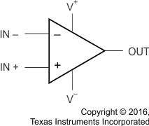 Figure 32. (Each Amplifier)
7.3 Feature Description
The amplifier's differential inputs consist of a non-inverting input (+IN) and an inverting input (–IN). The amplifer amplifies only the difference in voltage between the two inpus, which is called the differential input voltage. The output voltage of the op-amp Vout is given by Equation 1:
where AOL is the open-loop gain of the amplifier, typically around 100dB (100,000x, or 10uV per Volt).
7.4 Device Functional Modes
This section covers the following design considerations:
1. Frequency and Phase Response Considerations
2. Unity-Gain Pulse Response Considerations
3. Input Bias Current Considerations
7.4.1 Frequency and Phase Response Considerations
The relationship between open-loop frequency response and open-loop phase response determines the closed-loop stability performance (negative feedback). The open-loop phase response causes the feedback signal to shift towards becoming positive feedback, thus becoming unstable. The further the output phase angle is from the input phase angle, the more stable the negative feedback will operate. Phase Margin (φm) specifies this output-to-input phase relationship at the unity-gain crossover point. Zero degrees of phase-margin means that the input and output are completely in phase with each other and will sustain oscillation at the unity-gain frequency.
The AC tables show φm for a no load condition. But φm changes with load. The Gain and Phase margin vs Frequency plots in the curve section can be used to graphically determine the φm for various loaded conditions. To do this, examine the phase angle portion of the plot, find the phase margin point at the unity-gain frequency, and determine how far this point is from zero degree of phase-margin. The larger the phase-margin, the more stable the circuit operation.
The bandwidth is also affected by load. The graphs of Figure 33 and Figure 34 provide a quick look at how various loads affect the φm and the bandwidth of the LMV821/822/824 family. These graphs show capacitive loads reducing both φm and bandwidth, while resistive loads reduce the bandwidth but increase the φm. Notice how a 600Ω resistor can be added in parallel with 220 picofarads capacitance, to increase the φm 20°(approx.), but at the price of about a 100 kHz of bandwidth.
Overall, the LMV821/822/824 family provides good stability for loaded condition.
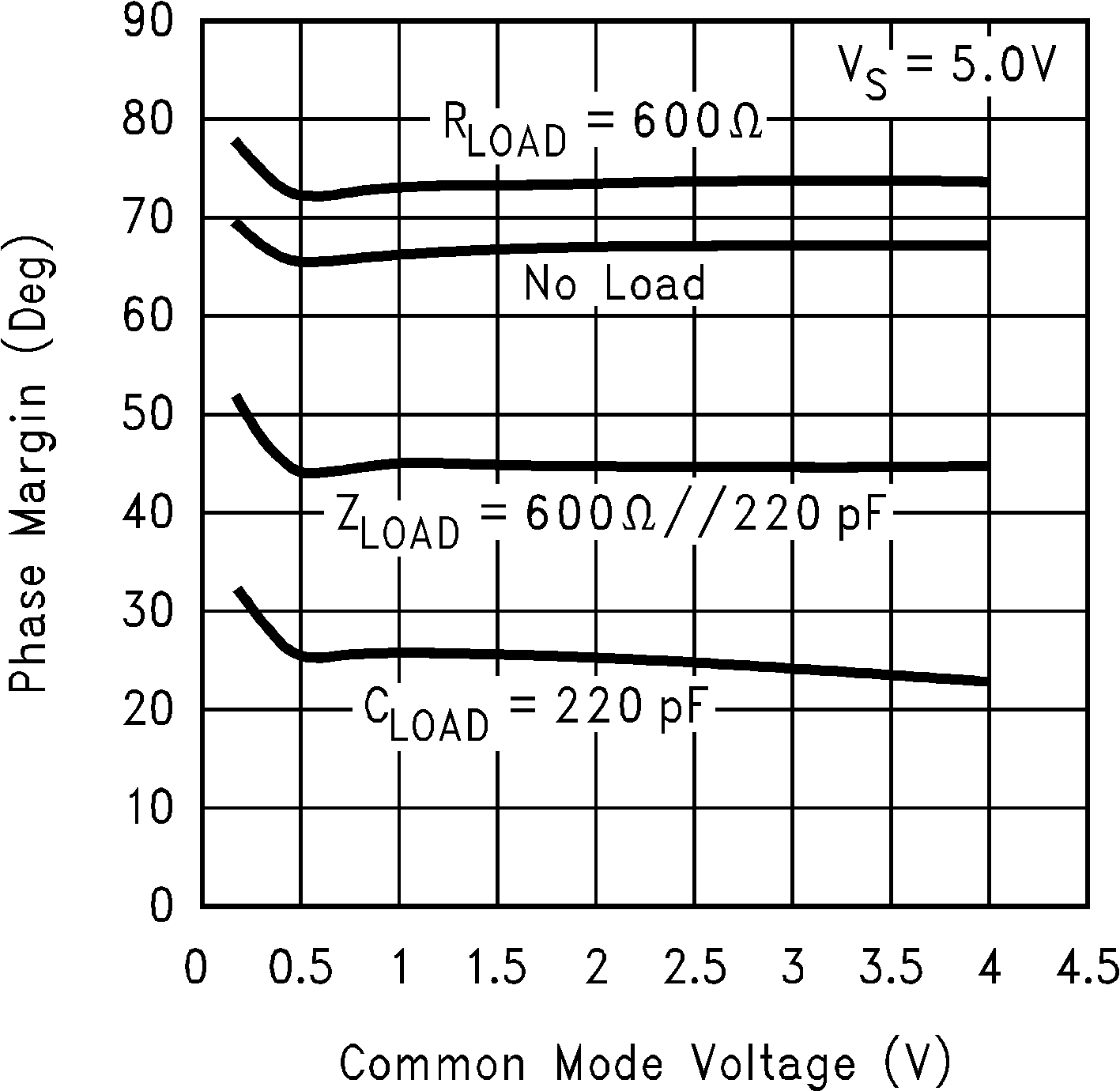 Figure 33. Phase Margin vs Common Mode Voltage for Various Loads
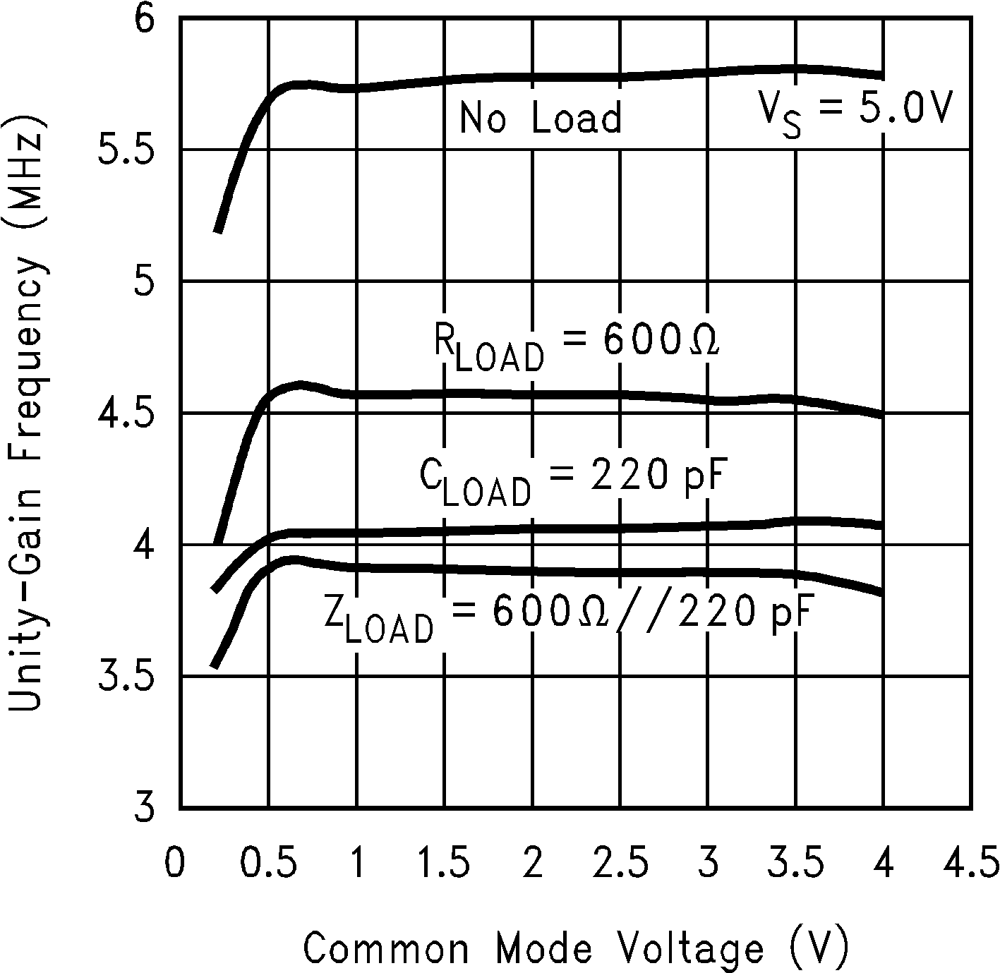 Figure 34. Unity-Gain Frequency vs Common Mode Voltage for Various Loads
7.4.2 Unity Gain Pulse Response Consideration
A pull-up resistor is well suited for increasing unity-gain, pulse response stability. For example, a 600 Ω pull-up resistor reduces the overshoot voltage by about 50%, when driving a 220 pF load. Figure 35 shows how to implement the pull-up resistor for more pulse response stability.
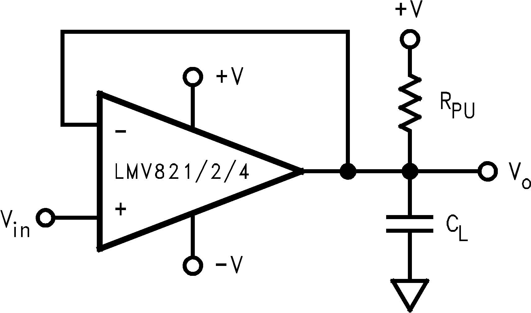 Figure 35. Using a Pull-up Resistor at the Output for Stabilizing Capacitive Loads
Higher capacitances can be driven by decreasing the value of the pull-up resistor, but its value shouldn't be reduced beyond the sinking capability of the part. An alternate approach is to use an isolation resistor as illustrated in Figure 36.
Figure 37 shows the resulting pulse response from a LMV824, while driving a 10,000 pF load through a 20Ω isolation resistor.
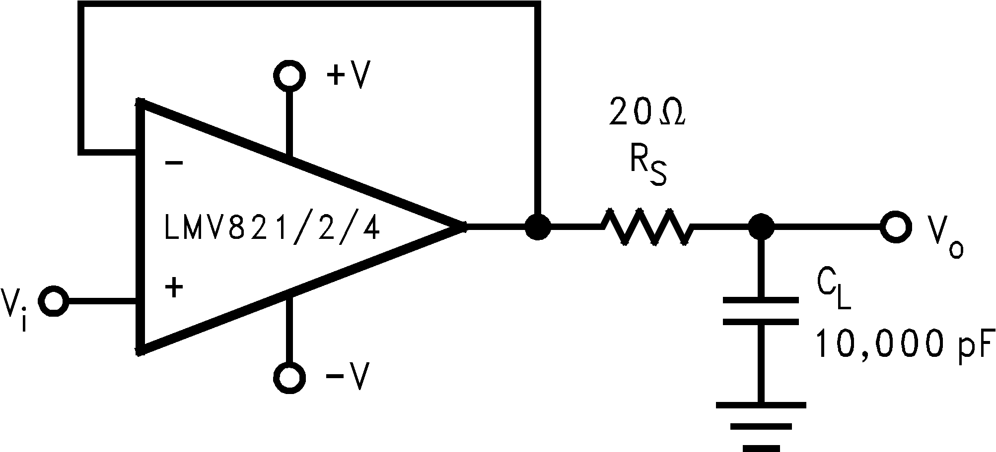 Figure 36. Using an Isolation Resistor to Drive Heavy Capacitive Loads
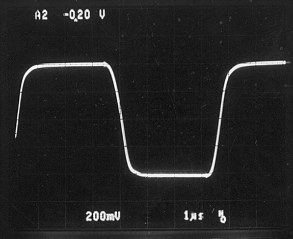 Figure 37. Pulse Response per Figure 36
7.4.3 Input Bias Current Consideration
Input bias current (IB) can develop a somewhat significant offset voltage. This offset is primarily due to IB flowing through the negative feedback resistor, RF. For example, if IB is 90 nA (max @ room) and RF is 100 kΩ, then an offset of 9 mV will be developed (VOS= IB x RF).Using a compensation resistor (RC), as shown in Figure 38, cancels out this affect. But the input offset current (IOS) will still contribute to an offset voltage in the same manner - typically 0.05 mV at room temp.
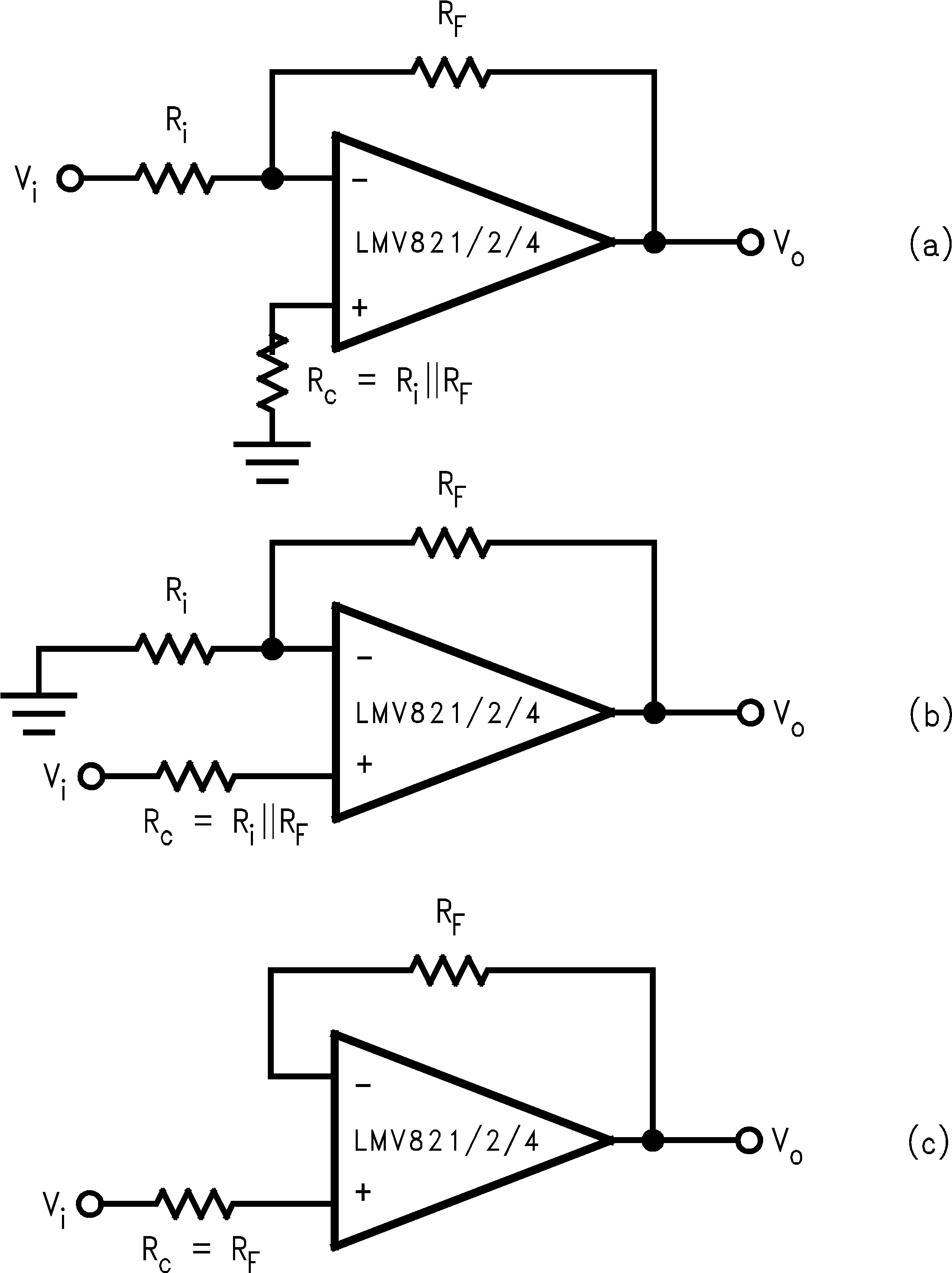 Figure 38. Canceling the Voltage Offset Effect of Input Bias Current