SNOSD79 October 2017 LMV841-Q1 , LMV842-Q1 , LMV844-Q1
PRODUCTION DATA.
- 1 Features
- 2 Applications
- 3 Description
- 4 Revision History
- 5 Pin Configuration and Functions
- 6 Specifications
- 7 Detailed Description
- 8 Application and Implementation
- 9 Power Supply Recommendations
- 10Layout
- 11Device and Documentation Support
- 12Mechanical, Packaging, and Orderable Information
- 12机械、封装和可订购信息
Package Options
Mechanical Data (Package|Pins)
- DCK|5
Thermal pad, mechanical data (Package|Pins)
Orderable Information
7 Detailed Description
7.1 Overview
The LMV84x-Q1 devices are operational amplifiers with near-precision specifications: low noise, low temperature drift, low offset, and rail-to-rail input and output. Possible application areas include instrumentation, medical, test equipment, audio, and automotive applications.
Its low supply current of 1 mA per amplifier, temperature range of −40°C to +125°C, 12-V supply with CMOS input, and the small SC70 package for the LMV841-Q1 make the LMV84x-Q1 a unique op amp family and a perfect choice for portable electronics.
7.2 Functional Block Diagram
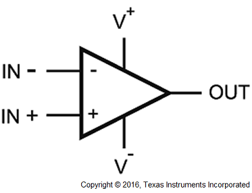
7.3 Feature Description
7.3.1 Input Protection
The LMV84x-Q1 devices have a set of anti-parallel diodes D1 and D2 between the input pins, as shown in Figure 34. These diodes are present to protect the input stage of the amplifier. At the same time, they limit the amount of differential input voltage that is allowed on the input pins.
A differential signal larger than one diode voltage drop can damage the diodes. The differential signal between the inputs needs to be limited to ±300 mV or the input current needs to be limited to ±10 mA.
NOTE
When the op amp is slewing, a differential input voltage exists that forward-biases the protection diodes. This may result in current being drawn from the signal source. While this current is already limited by the internal resistors R1 and R2 (both 130 Ω), a resistor of 1 kΩ can be placed in the feedback path, or a 500-Ω resistor can be placed in series with the input signal for further limitation.
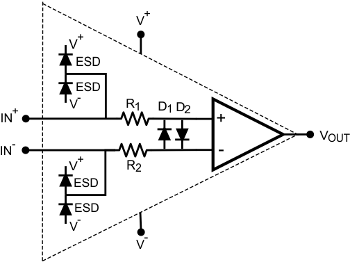 Figure 34. Protection Diodes Between the Input Pins
7.3.2 Input Stage
The input stage of this amplifier consists of both a PMOS and an NMOS input pair to achieve a rail-to-rail input range. For input voltages close to the negative rail, only the PMOS pair is active. Close to the positive rail, only the NMOS pair is active. In a transition region that extends from approximately 2 V below V+ to 1 V below V+, both pairs are active, and one pair gradually takes over from the other. In this transition region, the input-referred offset voltage changes from the offset voltage associated with the PMOS pair to that of the NMOS pair. The input pairs are trimmed independently to ensure an input offset voltage of less then 0.5 mV at room temperature over the complete rail-to-rail input range. This also significantly improves the CMRR of the amplifier in the transition region.
NOTE
The CMRR and PSRR limits in the tables are large-signal numbers that express the maximum variation of the input offset of the amplifier over the full common-mode voltage and supply voltage range, respectively. When the common-mode input voltage of the amplifier is within the transition region, the small signal CMRR and PSRR may be slightly lower than the large signal limits.
7.4 Device Functional Modes
7.4.1 Driving Capacitive Load
The LMV84x-Q1 can be connected as noninverting unity gain amplifiers. This configuration is the most sensitive to capacitive loading. The combination of a capacitive load placed on the output of an amplifier along with the output impedance of the amplifier creates a phase lag, which reduces the phase margin of the amplifier. If the phase margin is significantly reduced, the response is under-damped, which causes peaking in the transfer. When there is too much peaking, the op amp might start oscillating.
The LMV84x-Q1 can directly drive capacitive loads up to 100 pF without any stability issues. To drive heavier capacitive loads, an isolation resistor (RISO) must be used, as shown in Figure 35. By using this isolation resistor, the capacitive load is isolated from the output of the amplifier, and hence, the pole caused by CL is no longer in the feedback loop. The larger the value of RISO, the more stable the output voltage is. If values of RISO are sufficiently large, the feedback loop is stable, independent of the value of CL. However, larger values of RISO result in reduced output swing and reduced output current drive.
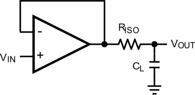 Figure 35. Isolating Capacitive Load
7.4.2 Noise Performance
The LMV84x-Q1 devices have good noise specifications and are frequently used in low-noise applications. Therefore it is important to determine the noise of the total circuit. Besides the input-referred noise of the op amp, the feedback resistors may have an important contribution to the total noise.
For applications with a voltage input configuration, in general it is beneficial general, beneficial to keep the resistor values low. In these configurations high resistor values mean high noise levels. However, using low resistor values will increase the power consumption of the application. This is not always acceptable for portable applications, so there is a trade-off between noise level and power consumption.
Besides the noise contribution of the signal source, three types of noise need to be taken into account for calculating the noise performance of an op amp circuit:
- Input-referred voltage noise of the op amp
- Input-referred current noise of the op amp
- Noise sources of the resistors in the feedback network, configuring the op amp
To calculate the noise voltage at the output of the op amp, the first step is to determine a total equivalent noise source. This requires the transformation of all noise sources to the same reference node. A convenient choice for this node is the input of the op amp circuit. The next step is to add all the noise sources. The final step is to multiply the total equivalent input voltage noise with the gain of the op amp configuration.
If the input-referred voltage noise of the op amp is already placed at the input, the user can use the input-referred voltage noise without further transferring. The input-referred current noise needs to be converted to an input-referred voltage noise. The current noise is negligibly small, as long as the equivalent resistance is not unrealistically large, so the user can leave the current noise out for these examples. That leaves the user with the noise sources of the resistors, being the thermal noise voltage. The influence of the resistors on the total noise can be seen in the following examples, one with high resistor values and one with low resistor values. Both examples describe an op amp configuration with a gain of 101 which gives the circuit a bandwidth of 44.5 kHz. The op amp noise is the same for both cases, that is, an input-referred noise voltage of 20 nV/ and a negligibly small input-referred noise current.
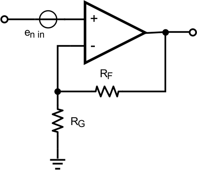 Figure 36. Noise Circuit
To calculate the noise of the resistors in the feedback network, the equivalent input-referred noise resistance is needed. For the example in Figure 36, this equivalent resistance Req can be calculated using Equation 1:

The voltage noise of the equivalent resistance can be calculated using Equation 2:

where
- enr = thermal noise voltage of the equivalent resistor
- Req (V/
 )
) - k = Boltzmann constant (1.38 x 10⁻²³ J/K)
- T = absolute temperature (K)
- Req = resistance (Ω)
The total equivalent input voltage noise is given by Equation 3:

where
- en in = total input equivalent voltage noise of the circuit
- env = input voltage noise of the op amp
The final step is multiplying the total input voltage noise by the noise gain using Equation 4, which is in this case the gain of the op amp configuration:

The equivalent resistance for the first example with a resistor RF of 10 MΩ and a resistor RG of 100 kΩ at 25°C (298 K) equals Equation 5:

Now the noise of the resistors can be calculated using Equation 6, yielding:

The total noise at the input of the op amp is calculated in Equation 7:

For the first example, this input noise, multiplied with the noise gain, in Equation 8 gives a total output noise of:

In the second example, with a resistor RF of 10 kΩ and a resistor RG of 100 Ω at 25°C (298 K), the equivalent resistance equals Equation 9:

The resistor noise for the second example is calculated in Equation 10:

The total noise at the input of the op amp is calculated in Equation 10:

For the second example the input noise, multiplied with the noise gain, in Equation 12 gives an output noise of:

In the first example the noise is dominated by the resistor noise due to the very high resistor values, in the second example the very low resistor values add only a negligible contribution to the noise and now the dominating factor is the op amp itself. When selecting the resistor values, it is important to choose values that do not add extra noise to the application. Choosing values above 100 kΩ may increase the noise too much. Low values keep the noise within acceptable levels; choosing very low values however, does not make the noise even lower, but can increase the current of the circuit.
7.5 Interfacing to High Impedance Sensor
With CMOS inputs, the LMV84x-Q1 are particularly suited to be used as high impedance sensor interfaces.
Many sensors have high source impedances that may range up to 10 MΩ. The input bias current of an amplifier loads the output of the sensor, and thus cause a voltage drop across the source resistance, as shown in Figure 37. When an op amp is selected with a relatively high input bias current, this error may be unacceptable.
The low input current of the LMV84x-Q1 significantly reduces such errors. The following examples show the difference between a standard op amp input and the CMOS input of the LMV84x-Q1.
The voltage at the input of the op amp can be calculated with Equation 13:
For a standard op amp, the input bias Ib can be 10 nA. When the sensor generates a signal of 1 V (VS) and the sensors impedance is 10 MΩ (RS), the signal at the op amp input is calculated in Equation 14:
For the CMOS input of the LMV84x-Q1, which has an input bias current of only 0.3 pA, this would give Equation 15:
The conclusion is that a standard op amp, with its high input bias current input, is not a good choice for use in impedance sensor applications. The LMV84x-Q1 devices, in contrast, are much more suitable due to the low input bias current. The error is negligibly small; therefore, the LMV84x-Q1 are a must for use with high-impedance sensors.
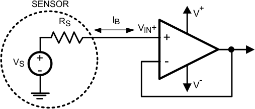 Figure 37. High Impedance Sensor Interface