SNOSD79 October   2017 LMV841-Q1 , LMV842-Q1 , LMV844-Q1

PRODUCTION DATA.  

  1. Features
  2. Applications
  3. Description
  4. Revision History
  5. Pin Configuration and Functions
  6. Specifications
    1. 6.1 Absolute Maximum Ratings
    2. 6.2 ESD Ratings
    3. 6.3 Recommended Operating Conditions
    4. 6.4 Thermal Information
    5. 6.5 Electrical Characteristics - 3.3 V
    6. 6.6 Electrical Characteristics - 5 V
    7. 6.7 Electrical Characteristics - ±5-V
    8. 6.8 Typical Characteristics
  7. Detailed Description
    1. 7.1 Overview
    2. 7.2 Functional Block Diagram
    3. 7.3 Feature Description
      1. 7.3.1 Input Protection
      2. 7.3.2 Input Stage
    4. 7.4 Device Functional Modes
      1. 7.4.1 Driving Capacitive Load
      2. 7.4.2 Noise Performance
    5. 7.5 Interfacing to High Impedance Sensor
  8. Application and Implementation
    1. 8.1 Application Information
    2. 8.2 Typical Applications
      1. 8.2.1 Active Filter Circuit
        1. 8.2.1.1 Design Requirements
        2. 8.2.1.2 Detailed Design Procedure
        3. 8.2.1.3 Application Curve
      2. 8.2.2 High-Side, Current-Sensing Circuit
        1. 8.2.2.1 Design Requirements
        2. 8.2.2.2 Detailed Design Procedure
      3. 8.2.3 Thermocouple Sensor Signal Amplification
        1. 8.2.3.1 Design Requirements
        2. 8.2.3.2 Detailed Design Procedure
  9. Power Supply Recommendations
  10. 10Layout
    1. 10.1 Layout Guidelines
    2. 10.2 Layout Example
  11. 11Device and Documentation Support
    1. 11.1 Related Links
    2. 11.2 Receiving Notification of Documentation Updates
    3. 11.3 Community Resources
      1. 11.5 静电放电警告
      2. 11.6 Glossary
    4. 11.4 Trademarks
    5. 11.5 Electrostatic Discharge Caution
    6. 11.6 Glossary
  12. 12Mechanical, Packaging, and Orderable Information
  13. 12机械、封装和可订购信息

Package Options

Mechanical Data (Package|Pins)
Thermal pad, mechanical data (Package|Pins)
Orderable Information

Pin Configuration and Functions

DCK Package
5-Pin SC70
Top View
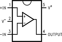
LMV841-Q1 LMV842-Q1 LMV844-Q1 20168302.png
D or DGK Package
8-Pin SOIC and VSSOP
Top View
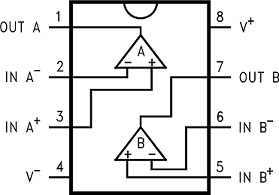
LMV841-Q1 LMV842-Q1 LMV844-Q1 20168303.png
D or PW Package
14-Pin SOIC and TSSOP
Top View
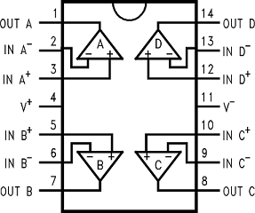
LMV841-Q1 LMV842-Q1 LMV844-Q1 20168304.png

Pin Functions

PIN DESCRIPTION
NAME I/O.
+IN I Noninverting Input
–IN I Inverting Input
OUT O Output
V+ P Positive Supply
V– P Negative Supply