SNVS677H May 2011 – October 2023 LMZ10501
PRODUCTION DATA
- 1
- 1 Features
- 2 Applications
- 3 Description
- 4 Revision History
- 5 Pin Configuration and Functions
- 6 Specifications
- 7 Detailed Description
- 8 Application and Implementation
- 9 Device and Documentation Support
- 10Mechanical, Packaging, and Orderable Information
Package Options
Refer to the PDF data sheet for device specific package drawings
Mechanical Data (Package|Pins)
- SIL|8
Thermal pad, mechanical data (Package|Pins)
Orderable Information
5 Pin Configuration and Functions
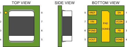
 Figure 5-1 SIL Package,8-PinµSIP
Table 5-1 Pin Functions
| PIN | TYPE(1) | DESCRIPTION | |
|---|---|---|---|
| NAME | NO. | ||
| EN | 1 | I | Enable Input. Set this digital input higher than 1.2 V for normal operation. For shutdown, set low. Pin is internally pulled up to VIN and can be left floating for always-on operation. |
| VCON | 2 | I | Output voltage control pin. Connect to analog voltage from resisitve divider or DAC/controller to set the VOUT voltage. VOUT = 2.5 x VCON. Connect a small (470pF) capacitor from this pin to SGND to provide noise filtering. |
| FB | 3 | I | Feedback of the error amplifier. Connect directly to output capacitor to sense VOUT. |
| SGND | 4 | I | Ground for analog and control circuitry. Connect to PGND at a single point. |
| VOUT | 5 | O | Output Voltage. Connected to one terminal of the integrated inductor. Connect output filter capacitor between VOUT and PGND. |
| PGND | 6 | I | Power ground for the power MOSFETs and gate-drive circuitry. |
| VIN | 7 | I | Voltage supply input. Connect ceramic capacitor between VIN and PGND as close as possible to these two pins. Typical capacitor values are between 4.7 µF and 22 µF. |
| VREF | 8 | O | 2.35-V voltage reference output. Typically connected to VCON pin through a resistive divider to set the output voltage. |
| PAD | I | The center pad underneath the SIL0008A package is internally tied to SGND. Connect this pad to the ground plane for improved thermal performance. | |
(1) I = input, O = output