SNVS670J June   2010  – April 2019 LMZ10504EXT

PRODUCTION DATA.  

  1. Features
  2. Applications
  3. Description
    1.     Device Images
      1.      Typical Application Circuit
      2.      Efficiency VOUT = 3.3 V
  4. Revision History
  5. Pin Configuration and Functions
    1.     Pin Functions
  6. Specifications
    1. 6.1 Absolute Maximum Ratings
    2. 6.2 ESD Ratings
    3. 6.3 Recommended Operating Conditions
    4. 6.4 Thermal Information
    5. 6.5 Electrical Characteristics
    6. 6.6 Typical Characteristics
  7. Detailed Description
    1. 7.1 Overview
    2. 7.2 Functional Block Diagram
    3. 7.3 Feature Description
      1. 7.3.1 Enable
      2. 7.3.2 Enable and UVLO
      3. 7.3.3 Soft-Start
      4. 7.3.4 Soft-Start Capacitor
      5. 7.3.5 Tracking
      6. 7.3.6 Tracking - Equal Soft-Start Time
      7. 7.3.7 Tracking - Equal Slew Rates
      8. 7.3.8 Current Limit
      9. 7.3.9 Overtemperature Protection
    4. 7.4 Device Functional Modes
      1. 7.4.1 Prebias Start-Up Capability
  8. Application and Implementation
    1. 8.1 Application Information
    2. 8.2 Typical Application
      1. 8.2.1 Design Requirements
      2. 8.2.2 Detailed Design Procedure
        1. 8.2.2.1 Custom Design With WEBENCH® Tools
        2. 8.2.2.2 Input Capacitor Selection
        3. 8.2.2.3 Output Capacitor Selection
          1. 8.2.2.3.1 Output Voltage Setting
        4. 8.2.2.4 Loop Compensation
      3. 8.2.3 Application Curves
    3. 8.3 System Examples
      1. 8.3.1 Application Schematic for 3.3-V to 5-V Input and 2.5-V Output With Optimized Ripple and Transient Response
      2. 8.3.2 Application Schematic for 3.3-V to 5-V Input and 2.5-V Output
      3. 8.3.3 EMI Tested Schematic for 2.5-V Output Based on 3.3-V to 5-V Input
  9. Power Supply Recommendations
  10. 10Layout
    1. 10.1 Layout Guidelines
    2. 10.2 Layout Examples
    3. 10.3 Estimate Power Dissipation and Thermal Considerations
    4. 10.4 Power Module SMT Guidelines
  11. 11Device and Documentation Support
    1. 11.1 Device Support
      1. 11.1.1 Third-Party Products Disclaimer
      2. 11.1.2 Development Support
        1. 11.1.2.1 Custom Design With WEBENCH® Tools
    2. 11.2 Documentation Support
      1. 11.2.1 Related Documentation
    3. 11.3 Receiving Notification of Documentation Updates
    4. 11.4 Community Resources
    5. 11.5 Trademarks
    6. 11.6 Electrostatic Discharge Caution
    7. 11.7 Glossary
  12. 12Mechanical, Packaging, and Orderable Information

Package Options

Mechanical Data (Package|Pins)
Thermal pad, mechanical data (Package|Pins)
Orderable Information

Typical Application

This section provides several application solutions with an associated bill of materials. The compensation for each solution was optimized to work over the full input range. Many applications have a fixed input voltage rail. It is possible to modify the compensation to obtain a faster transient response for a given input voltage operating point.
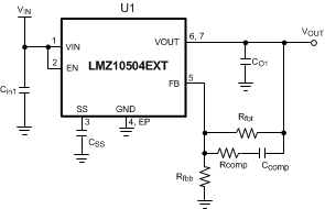
LMZ10504EXT 30118454.gifFigure 21. Typical Application Schematic