SNVS633K January   2010  – April 2019 LMZ10505

PRODUCTION DATA.  

  1. Features
  2. Applications
  3. Description
    1.     Device Images
      1.      Typical Application Circuit
      2.      Efficiency VOUT = 3.3 V
  4. Revision History
  5. Pin Configuration and Functions
    1.     Pin Functions
  6. Specifications
    1. 6.1 Absolute Maximum Ratings
    2. 6.2 ESD Ratings
    3. 6.3 Recommended Operating Conditions
    4. 6.4 Thermal Information
    5. 6.5 Electrical Characteristics
    6. 6.6 Typical Characteristics
  7. Detailed Description
    1. 7.1 Overview
    2. 7.2 Functional Block Diagram
    3. 7.3 Feature Description
      1. 7.3.1 Enable
      2. 7.3.2 Enable and UVLO
      3. 7.3.3 Soft-Start
      4. 7.3.4 Soft-Start Capacitor
      5. 7.3.5 Tracking
      6. 7.3.6 Tracking - Equal Soft-Start Time
      7. 7.3.7 Tracking - Equal Slew Rates
      8. 7.3.8 Current Limit
      9. 7.3.9 Overtemperature Protection
    4. 7.4 Device Functional Modes
      1. 7.4.1 Prebias Start-Up Capability
  8. Application and Implementation
    1. 8.1 Application Information
    2. 8.2 Typical Application
      1. 8.2.1 Design Requirements
      2. 8.2.2 Detailed Design Procedure
        1. 8.2.2.1 Custom Design With WEBENCH® Tools
        2. 8.2.2.2 Input Capacitor Selection
        3. 8.2.2.3 Output Capacitor Selection
          1. 8.2.2.3.1 Output Voltage Setting
        4. 8.2.2.4 Loop Compensation
      3. 8.2.3 Application Curves
    3. 8.3 System Examples
      1. 8.3.1 Application Schematic for 3.3-V to 5-V Input and 2.5-V Output With Optimized Ripple and Transient Response
      2. 8.3.2 Application Schematic for 3.3-V to 5-V Input and 2.5-V Output
      3. 8.3.3 EMI Tested Schematic for 2.5-V Output Based on 3.3-V to 5-V Input
  9. Power Supply Recommendations
  10. 10Layout
    1. 10.1 Layout Guidelines
    2. 10.2 Layout Examples
    3. 10.3 Estimate Power Dissipation and Thermal Considerations
    4. 10.4 Power Module SMT Guidelines
  11. 11Device and Documentation Support
    1. 11.1 Device Support
      1. 11.1.1 Third-Party Products Disclaimer
      2. 11.1.2 Development Support
        1. 11.1.2.1 Custom Design With WEBENCH® Tools
    2. 11.2 Documentation Support
      1. 11.2.1 Related Documentation
    3. 11.3 Receiving Notification of Documentation Updates
    4. 11.4 Community Resources
    5. 11.5 Trademarks
    6. 11.6 Electrostatic Discharge Caution
    7. 11.7 Glossary
  12. 12Mechanical, Packaging, and Orderable Information

Package Options

Mechanical Data (Package|Pins)
Thermal pad, mechanical data (Package|Pins)
Orderable Information

Pin Configuration and Functions

NDW Package
7-Lead TO-PMOD
Top View
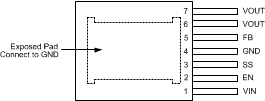
LMZ10505 30107472.gif

Pin Functions

PIN TYPE DESCRIPTION
NAME NO.
EN 2 Analog Active-high enable input for the device.
Exposed Pad Ground Exposed pad is used as a thermal connection to remove heat from the device. Connect this pad to the PCB ground plane in order to reduce thermal resistance value. EP must also provide a direct electrical connection to the input and output capacitors ground terminals. Connect EP to pin 4.
FB 5 Analog Feedback pin. This is the inverting input of the error amplifier used for sensing the output voltage. Keep the copper area of this node small.
GND 4 Ground Power ground and signal ground. Provide a direct connection to the EP. Place the bottom feedback resistor as close as possible to GND and FB pin.
SS 3 Analog Soft-start control pin. An internal 2-µA current source charges an external capacitor connected between SS and GND pins to set the output voltage ramp rate during start-up. The SS pin can also be used to configure the tracking feature.
VIN 1 Power Power supply input. A low-ESR input capacitance should be located as close as possible to the VIN pin and exposed pad (EP).
VOUT 6, 7 Power The output terminal of the internal inductor. Connect the output filter capacitor between VOUT pin and EP.