SNVS661G June 2010 – September 2015 LMZ12001EXT
PRODUCTION DATA.
- 1 Features
- 2 Applications
- 3 Description
- 4 Revision History
- 5 Pin Configuration and Functions
- 6 Specifications
- 7 Detailed Description
- 8 Application and Implementation
- 9 Power Supply Recommendations
- 10Layout
- 11Device and Documentation Support
- 12Mechanical, Packaging, and Orderable Information
Package Options
Mechanical Data (Package|Pins)
- NDW|7
Thermal pad, mechanical data (Package|Pins)
Orderable Information
5 Pin Configuration and Functions
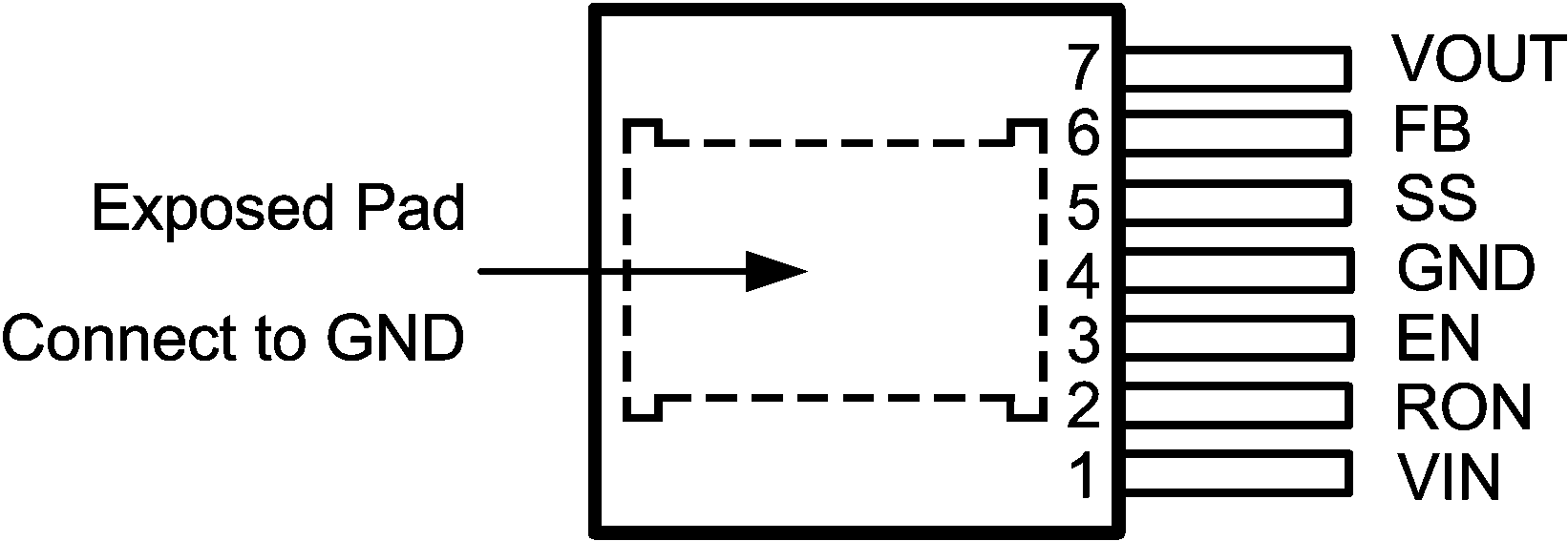
NDW Package
7-Pin
Top View

Pin Functions
| PIN | TYPE | DESCRIPTION | |
|---|---|---|---|
| NAME | NO. | ||
| EN | 3 | Analog | Enable — Input to the precision enable comparator. Rising threshold is 1.18-V nominal; 90-mV hysteresis nominal. Maximum recommended input level is 6.5 V. |
| EP | — | Ground | Exposed Pad — Internally connected to pin 4. Used to dissipate heat from the package during operation. Must be electrically connected to pin 4 external to the package. |
| FB | 6 | Analog | Feedback — Internally connected to the regulation, overvoltage, and short circuit comparators. The regulation reference point is 0.8 V at this input pin. Connected the feedback resistor divider between the output and ground to set the output voltage. |
| GND | 4 | Ground | Ground — Reference point for all stated voltages. Must be externally connected to EP. |
| RON | 2 | Analog | ON-Time Resistor — An external resistor from VIN to this pin sets the ON-time of the application. Typical values range from 25 kΩ to 124 kΩ. |
| SS | 5 | Analog | Soft-Start — An internal 8-µA current source charges an external capacitor to produce the soft-start function. This node is discharged at 200 µA during disable, overcurrent, thermal shutdown and internal UVLO conditions. |
| VIN | 1 | Power | Supply input — Nominal operating range is 4.5 V to 20 V. A small amount of internal capacitance is contained within the package assembly. Additional external input capacitance is required between this pin and exposed pad. |
| VOUT | 7 | Power | Output Voltage — Output from the internal inductor. Connect the output capacitor between this pin and exposed pad. |