SNVS648J January 2010 – October 2015 LMZ14202
PRODUCTION DATA.
- 1 Features
- 2 Applications
- 3 Description
- 4 Revision History
- 5 Pin Configuration and Functions
- 6 Specifications
- 7 Detailed Description
-
8 Application and Implementation
- 8.1 Application Information
- 8.2
Typical Application
- 8.2.1 Design Requirements
- 8.2.2 Detailed Design Procedure
- 8.2.3 Application Curves
- 9 Power Supply Recommendations
- 10Layout
- 11Device and Documentation Support
- 12Mechanical, Packaging, and Orderable Information
Package Options
Mechanical Data (Package|Pins)
- NDW|7
Thermal pad, mechanical data (Package|Pins)
Orderable Information
8 Application and Implementation
NOTE
Information in the following applications sections is not part of the TI component specification, and TI does not warrant its accuracy or completeness. TI’s customers are responsible for determining suitability of components for their purposes. Validate and test the design implementation to confirm system functionality.
8.1 Application Information
The LMZ14202 is a step-down DC-to-DC power module. It is typically used to convert a higher DC voltage to a lower DC voltage with a maximum output current of 2 A. The following design procedure can be used to select components for the LMZ14202. Alternately, the WEBENCH software may be used to generate complete designs.
WEBENCH software uses an iterative design procedure and accesses comprehensive databases of components. For more details, go to www.ti.com/WEBENCH.
8.2 Typical Application
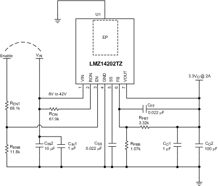 Figure 32. Evaluation Board Schematic Diagram
8.2.1 Design Requirements
For this example the following application parameters exist.
- VIN range: up to 42 V
- VOUT = 0.8 V to 5 V
- IOUT = 2 A
Refer to Table 2 for more information.
Table 1. Component Value Combinations
| VOUT (V) | RFBT (kΩ) | RFBB (kΩ) | RDS(on) (kΩ) | VIN (V) | |
|---|---|---|---|---|---|
| MIN | MAX | ||||
| 5 | 5.62 | 1.07 | 100 | 7.5 | 42 |
| 3.3 | 3.32 | 61.9 | 6 | 42 | |
| 2.5 | 2.26 | 47.5 | 30 | ||
| 1.8 | 1.87 | 1.5 | 32.4 | 25 | |
| 1.5 | 1 | 1.13 | 28 | 21 | |
| 1.2 | 4.22 | 8.45 | 22.6 | 19 | |
| 0.8 | 0 | 39.2 | 24.9 | 18 | |
Table 2. List of Materials
| REF DES | DESCRIPTION | SIZE | MANUFACTURER | PART NUMBER |
|---|---|---|---|---|
| U1 | SIMPLE SWITCHER | PFM-7 | Texas Instruments | LMZ14202TZ |
| CIN1 | 1 µF, 50 V, X7R | 1206 | Taiyo Yuden | UMK316B7105KL-T |
| CIN2 | 10 µF, 50 V, X7R | 1210 | Taiyo Yuden | UMK325BJ106MM-T |
| CO1 | 1 µF, 50 V, X7R | 1206 | Taiyo Yuden | UMK316B7105KL-T |
| CO2 | 100 µF, 6.3 V, X7R | 1210 | Taiyo Yuden | JMK325BJ107MM-T |
| RFBT | 3.32 kΩ | 0603 | Vishay Dale | CRCW06033K32FKEA |
| RFBB | 1.07 kΩ | 0603 | Vishay Dale | CRCW06031K07FKEA |
| RDS(on) | 61.9 kΩ | 0603 | Vishay Dale | CRCW060361k9FKEA |
| RENT | 68.1 kΩ | 0603 | Vishay Dale | CRCW060368k1FKEA |
| RENB | 11.8 kΩ | 0603 | Vishay Dale | CRCW060311k8FKEA |
| CFF | 22 nF, ±10%, X7R, 16 V | 0603 | TDK | C1608X7R1H223K |
| CSS | 22 nF, ±10%, X7R, 16 V | 0603 | TDK | C1608X7R1H223K |
8.2.2 Detailed Design Procedure
8.2.2.1 Design Steps for the LMZ14202 Application
The LMZ14202 is fully supported by WEBENCH and offers the following: Component selection, electrical and thermal simulations as well as the build-it board for a reduction in design time. The following list of steps can be used to manually design the LMZ14202 application.
- Select minimum operating VIN with enable divider resistors
- Program VO with divider resistor selection
- Program turnon time with soft-start capacitor selection
- Select CO
- Select CIN
- Set operating frequency with RDS(on)
- Determine module dissipation
- Carefully consider thermal performance required when designing the PCB layout
8.2.2.1.1 Enable Divider, RENT and RENB Selection
The enable input provides a precise, 1.18-V band-gap rising threshold to allow direct logic drive or connection to a voltage divider from a higher enable voltage such as VIN. The enable input also incorporates 90 mV (typical) of hysteresis resulting in a falling threshold of 1.09 V. The maximum recommended voltage into the EN pin is 6.5 V. For applications where the midpoint of the enable divider exceeds 6.5 V, a small Zener diode can be added to limit this voltage.
The function of this resistive divider is to allow the designer to choose an input voltage below which the circuit becomes disabled. This implements the feature of programmable undervoltage lockout. This is often used in battery powered systems to prevent deep discharge of the system battery. It is also useful in system designs for sequencing of output rails or to prevent early turnon of the supply as the main input voltage rail rises at power-up. Applying the enable divider to the main input rail is often done in the case of higher input voltage systems such as 24-V AC/DC systems where a lower boundary of operation must be established. In the case of sequencing supplies, the divider is connected to a rail that becomes active earlier in the power-up cycle than the LMZ14202 output rail. Choose the two resistors based on Equation 1.
The LMZ14202 demonstration and evaluation boards use 11.8 kΩ for RENB and 68.1 kΩ for RENT resulting in a rising UVLO of 8 V. This divider presents 6.25 V to the EN input when the divider input is raised to 42 V.
The EN pin is internally pulled up to VIN and can be left floating for always-on operation.
8.2.2.1.2 Output Voltage Selection
Output voltage is determined by a divider of two resistors connected between VO and ground. The midpoint of the divider is connected to the FB input. The voltage at FB is compared to a 0.8-V internal reference. In normal operation an ON-time cycle is initiated when the voltage on the FB pin falls below 0.8 V. The main MOSFET ON-time cycle causes the output voltage to rise and the voltage at the FB to exceed 0.8 V. As long as the voltage at FB is above 0.8 V, ON-time cycles does not occur.
The regulated output voltage determined by the external divider resistors RFBT and RFBB is:
Rearranging terms; the ratio of the feedback resistors for a desired output voltage is:
Choose these resistors from values between 1 kΩ and 10 kΩ.
For VO = 0.8 V the FB pin can be connected to the output directly so long as an output preload resistor remains that draws more than 20 µA. Converter operation requires this minimum load to create a small inductor ripple current and maintain proper regulation when no load is present.
A feed-forward capacitor is placed in parallel with RFBT to improve load step transient response. Its value is usually determined experimentally by load stepping between DCM and CCM conduction modes and adjusting for best transient response and minimum output ripple.
A table of values for RFBT , RFBB , CFF and RDS(on) is included in the applications schematic.
8.2.2.1.3 Soft-Start Capacitor Selection
Programmable soft-start permits the regulator to slowly ramp to its steady state operating point after being enabled, thereby reducing current inrush from the input supply and slowing the output voltage rise-time to prevent overshoot.
Upon turnon, after all UVLO conditions have been passed, an internal 8 µA current source begins charging the external soft-start capacitor. The soft-start time duration to reach steady state operation is given by the formula:
This equation can be rearranged as follows:
Use of a 0.022-μF capacitor results in 2.2-ms soft-start duration which is recommended as a minimum value.
As the soft-start input exceeds 0.8 V the output of the power stage comes into regulation. The soft-start capacitor continues charging until it reaches approximately 3.8 V on the SS pin. Voltage levels between 0.8 V and 3.8 V have no effect on other circuit operation. The following conditions reset the soft-start capacitor by discharging the SS input to ground with an internal 200-μA current sink.
- The enable input being pulled low
- Thermal shutdown condition
- Over-current fault
- Internal VCC UVLO (approximately 4-V input to VIN)
8.2.2.1.4 CO Selection
None of the required CO output capacitance is contained within the module. At a minimum, the output capacitor must meet the worst-case minimum ripple current rating of 0.5 × ILR(P-P), as calculated in Equation 17 below. Beyond the worst-case minimum, additional capacitance reduces output ripple as long as the ESR is low enough to permit it. A minimum value of 10 μF is generally required. Expect to experiment when designing an application to operate with a minimum value. Ceramic capacitors or other low ESR types are recommended. See AN-2024 LMZ1420x / LMZ1200x Evaluation Board (SNVA422) for more detail.
Equation 6 provides a good first-pass approximation of CO for load transient requirements:
Solving:
The LMZ14202 demonstration and evaluation boards are populated with a 100-µF 6.3-V X5R output capacitor. Locations for extra output capacitors are provided. See See AN-2024 LMZ1420x / LMZ1200x Evaluation Board (SNVA422) for locations.
8.2.2.1.5 Input Capacitance (CIN) Selection
The LMZ14202 module contains an internal 0.47-µF input ceramic capacitor. Additional input capacitance is required external to the module to handle the input ripple current of the application. This input capacitance must be very close to the module. Input capacitor selection is generally directed to satisfy the input ripple current requirements rather than by capacitance value. Worst-case input ripple current rating is dictated by Equation 8:

where
- D ≊ VO / VIN
The worst-case ripple current occurs when the module is presented with full load current and when VIN = (2 × VO).
Recommended minimum input capacitance is 10-µF X7R ceramic with a voltage rating at least 25% higher than the maximum applied input voltage for the application. TI also recommends to pay attention to the voltage and temperature deratings of the capacitor selected.
NOTE
If the capacitor data sheet omits ripple current rating of the ceramic capacitors, contact the capacitor manufacturer to obtain this rating.
If the system design requires a certain minimum value of input ripple voltage ΔVIN be maintained then Equation 9 may be used.
If ΔVIN is 1% of VIN for a 24V input to 3.3V output application this equals 240 mV and fSW = 400 kHz.
CIN≥ 2 A × 3.3 V / 24V × (1– 3.3 V/24 V) / (400000 × 0.240 V)
≥ 2.5 μF
Additional bulk capacitance with higher ESR may be required to damp any resonant effects of the input capacitance and parasitic inductance of the incoming supply lines.
8.2.2.1.6 RDS(on) Resistor Selection
Many designs begin with a desired switching frequency in mind. For that purpose Equation 10 can be used.
This can be rearranged as
The selection of RON and fSW(CCM) must be confined by limitations in the ON-time and OFF-time for the Constant On-Time Control (COT) Circuit Overview section.
The ON-time of the LMZ14202 timer is determined by the resistor RDS(on) and the input voltage VIN. It is calculated as follows:
The inverse relationship of tON and VIN gives a nearly constant switching frequency as VIN is varied. Select an RDS(on) level to fascilitate an ON-time at maximum VIN is greater than 150 ns. The ON-timer has a limiter to ensure a minimum of 150 ns for tON. This function imits the maximum operating frequency, which is governed by Equation 13:
Use Equation 14 to select RDS(on) a particular operating frequency while maintaining the minimum ON-time of 150 ns.
If RDS(on) calculated in Equation 11 is less than the minimum value determined in Equation 14, select a lower frequency. Alternatively, VIN(max) can also be limited to keep the frequency unchanged.
NOTE
The minimum OFF-time of 260 ns limits the maximum duty ratio. Select a larger RDS(on) (lower fSW) for any application requiring large duty ratio.
8.2.2.1.6.1 Discontinuous Conduction and Continuous Conduction Mode Selection
Operating frequency in DCM can be calculated as follows:
In CCM, current flows through the inductor through the entire switching cycle and never falls to zero during the OFF-time. The switching frequency remains relatively constant with load current and line voltage variations. The CCM operating frequency can be calculated using Equation 7 above.
Following is a comparison pair of waveforms of the showing both CCM (upper) and DCM operating modes.
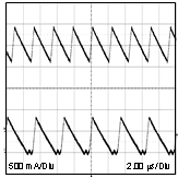 Figure 33. CCM and DCM Operating Modes
 VIN = 24 V, VO = 3.3 V, IO = 2 A/0.32 A 2 μs/div
The approximate formula for determining the DCM/CCM boundary is as follows:
Following is a typical waveform showing the boundary condition.
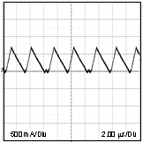 Figure 34. Transition Mode Operation
VIN = 24 V, VO = 3.3 V, IO = 0.35 A 2 μsec/div
The inductor internal to the module is 10 μH. This value was chosen as a good balance between low and high input voltage applications. The main parameter affected by the inductor is the amplitude of the inductor ripple current (ILR). ILR can be calculated with:
where
- VIN is the maximum input voltage and fSW is determined from Equation 10.
If the output current IO is determined by assuming that IO = IL, the higher and lower peak of ILR can be determined. Be aware that the lower peak of ILR must be positive if CCM operation is required.
8.2.3 Application Curves
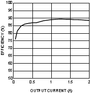 Figure 35. Efficiency VIN = 24 V VOUT = 5 V
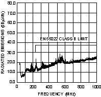 Figure 37. Radiated Emissions (EN 55022 Class B)
From Evaluation Board
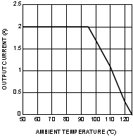 Figure 36. Thermal Derating Curve
VIN = 24 V, VOUT = 5 V,