SNVS872D August   2012  – August 2018 LMZ21700

PRODUCTION DATA.  

  1. Features
  2. Applications
  3. Description
    1.     Device Images
      1.      Simplified Schematic
      2.      Efficiency for VIN = 12 V
  4. Revision History
  5. Pin Configuration and Functions
    1.     Pin Functions
  6. Specifications
    1. 6.1 Absolute Maximum Ratings
    2. 6.2 ESD Ratings
    3. 6.3 Recommended Operating Conditions
    4. 6.4 Thermal Information
    5. 6.5 Electrical Characteristics
    6. 6.6 Typical Characteristics
  7. Detailed Description
    1. 7.1 Overview
    2. 7.2 Functional Block Diagram
      1. 7.2.1 Package Construction
    3. 7.3 Feature Description
      1. 7.3.1 Input Undervoltage Lockout
      2. 7.3.2 Enable Input (EN)
      3. 7.3.3 Soft-Start and Tracking Function (SS)
      4. 7.3.4 Power Good Function (PG)
      5. 7.3.5 Output Voltage Setting
      6. 7.3.6 Output Current Limit and Output Short Circuit Protection
      7. 7.3.7 Thermal Protection
    4. 7.4 Device Functional Modes
      1. 7.4.1 PWM Mode Operation
      2. 7.4.2 PSM Operation
  8. Application and Implementation
    1. 8.1 Application Information
    2. 8.2 Typical Application
      1. 8.2.1 Design Requirements
      2. 8.2.2 Detailed Design Procedure
        1. 8.2.2.1 Custom Design With WEBENCH® Tools
        2. 8.2.2.2 Input Capacitor (CIN)
        3. 8.2.2.3 Output Capacitor (COUT)
        4. 8.2.2.4 Softstart Capacitor (CSS)
        5. 8.2.2.5 Power Good Resistor (RPG)
        6. 8.2.2.6 Feedback Resistors (RFBB and RFBT)
      3. 8.2.3 Application Curves
        1. 8.2.3.1 VOUT = 1.2 V
        2. 8.2.3.2 VOUT = 1.8 V
        3. 8.2.3.3 VOUT = 2.5 V
        4. 8.2.3.4 VOUT = 3.3 V
        5. 8.2.3.5 VOUT = 5.0 V
    3. 8.3 Do's and Don'ts
  9. Power Supply Recommendations
    1. 9.1 Voltage Range
    2. 9.2 Current Capability
    3. 9.3 Input Connection
      1. 9.3.1 Voltage Drops
      2. 9.3.2 Stability
  10. 10Layout
    1. 10.1 Layout Guidelines
      1. 10.1.1 Minimize the High di/dt Loop Area
      2. 10.1.2 Protect the Sensitive Nodes in the Circuit
      3. 10.1.3 Provide Thermal Path and Shielding
    2. 10.2 Layout Example
      1. 10.2.1 High Density Layout Example for Space Constrained Applications
        1. 10.2.1.1 35-mm² Solution Size (Single Sided)
  11. 11Device and Documentation Support
    1. 11.1 Device Support
    2. 11.2 Development Support
      1. 11.2.1 Custom Design With WEBENCH® Tools
    3. 11.3 Receiving Notification of Documentation Updates
    4. 11.4 Community Resources
    5. 11.5 Trademarks
    6. 11.6 Electrostatic Discharge Caution
    7. 11.7 Glossary
  12. 12Mechanical, Packaging, and Orderable Information
    1. 12.1 Tape and Reel Information

Package Options

Refer to the PDF data sheet for device specific package drawings

Mechanical Data (Package|Pins)
  • SIL|8
Thermal pad, mechanical data (Package|Pins)
Orderable Information

Package Construction

In order to achieve a small solution size the LMZ21700 Nano Module comes in an innovative MicroSiP™ package. The construction consists of a synchronous buck converter IC embedded inside an FR-4 laminate substrate, with a power inductor mounted on top of the substrate material. See Figure 12 and Figure 13 below. The bottom (landing pads) of the package resemble a typical 8-pin DFN package. See the Mechanical drawings at the end of the datasheet for details on the recommended landing pattern and solder paste stencil information.
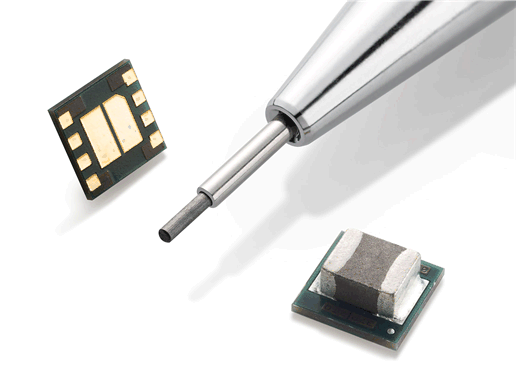
LMZ21700 SIL0008_PENCIL.gifFigure 12. LMZ21700 in the SIL0008E Package
LMZ21700 SIL0008_CONSTRUCTION2.gifFigure 13. LMZ21700 Package Construction Cross Section
(Illustration Only, Not to Scale)