SNVS707G March 2011 – August 2016 LMZ23610
PRODUCTION DATA.
- 1 Features
- 2 Applications
- 3 Description
- 4 Revision History
- 5 Pin Configuration and Functions
- 6 Specifications
- 7 Detailed Description
- 8 Application and Implementation
- 9 Power Supply Recommendations
- 10Layout
- 11Device and Documentation Support
- 12Mechanical, Packaging, and Orderable Information
Package Options
Mechanical Data (Package|Pins)
- NDY|11
Thermal pad, mechanical data (Package|Pins)
Orderable Information
7 Detailed Description
7.1 Overview
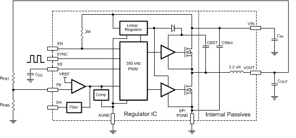
The architecture used is an internally compensated emulated peak current mode control, based on a monolithic synchronous SIMPLE SWITCHER core capable of supporting high load currents. The output voltage is maintained through feedback compared with an internal 0.8-V reference. For emulated peak current-mode, the valley current is sampled on the down-slope of the inductor current. This is used as the DC value of current to start the next cycle.
The primary application for emulated peak current-mode is high input voltage to low output voltage operating at a narrow duty cycle. By sampling the inductor current at the end of the switching cycle and adding an external ramp, the minimum ON-time can be significantly reduced, without the need for blanking or filtering which is normally required for peak current-mode control.
7.2 Functional Block Diagram
7.3 Feature Description
7.3.1 Synchronization Input
The PWM switching frequency can be synchronized to an external frequency source. The PWM switching will be in phase with the external frequency source. If this feature is not used, connect this input either directly to ground, or connect to ground through a resistor of 1.5 kΩ or less. The allowed synchronization frequency range is 314 kHz to 600 kHz. The typical input threshold is 1.4 V. Ideally, the input clock must overdrive the threshold by a factor of 2, so direct drive from 3.3-V logic through a 1.5-kΩ or less Thevenin source resistance is recommended. Note that applying a sustained logic 1 corresponds to 0-Hz PWM frequency and will cause the module to stop switching.
7.3.2 Current Sharing
When a load current higher than 10 A is required by the application, the LMZ23610 can be configured to share the load between multiple devices. To share the load current between the devices, connect the SH pin of all current sharing LMZ23610 modules. One device must be configured as the master by connecting FB normally. All other devices must be configured as slaves by leaving their respective FB pins floating. The modules must be synchronized by a clock signal to avoid beat frequencies in the output voltage caused by small differences in the internal 359-kHz clock. If the modules are not synchronized, the magnitude of the ripple voltage will depend on the phase relationship of the internal clocks. The external synchronizing clocks can be in phase for all modules, or out of phase to reduce the current stress on the input and output capacitors. As an example, two modules can be run 180 degrees out of phase, and three modules can be run 120 degrees out of phase. The VIN, VOUT, PGND, and AGND pins must also be connected with low impedance paths. It is particularly important to pay close attention to the layout of AGND and SH, as offsets in grounding or noise picked up from other devices will be seen as a mismatch in current sharing and could cause noise issues.
Current sharing modules can be configured to share the same set of bulk input and output capacitors, while each having their own local input and output bypass capacitors. A CIN_BYP >= 30 µF is still recommended for each module that is connected in a current sharing configuration. A COUT_BYP consisting of 47-nF X7R ceramic capacitor in parallel with a 22-µF ceramic capacitor is recommended to locally bypass the output voltage for each module. These capacitors will provide local bypassing of high-frequency switched currents.
In a current sharing system using two or more modules, the slaves have their error amp circuitry disconnected. The master overrides the error amplifier outputs of the slaves. This signal is then compared to each module’s individual current sense circuitry. Due to this, the current sense gain of the entire system increases according to the number of modules slaved to the master. To compensate for this and ensure good stability, the total output capacitance has to be increased. For example, two modules configured to provide 1.2 VOUT and 20 amps have a required total bulk output capacitance of COUT_BULK = 2 × 450-µF (ESR 25 mΩ). This is a thirty six percent increase in the required output capacitance of a stand alone module. Up to 6 modules can be connected in parallel for loads up to 60 A. For more information on current sharing refer to AN-2093 (SNVA460).
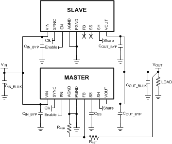 Figure 45. Current Sharing Example Schematic
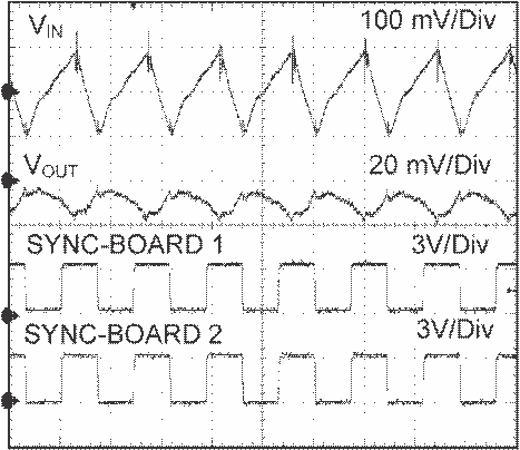
With Synchronization Clocks in Phase
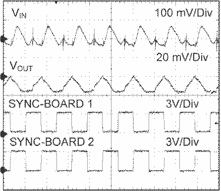
With Synchronization Clocks 180 Degrees Out of Phase
7.3.3 Output Overvoltage Protection
If the voltage at FB is greater than a 0.86-V internal reference, the output of the error amplifier is pulled toward ground, causing VOUT to fall.
7.3.4 Current Limit
The LMZ23610 is protected by both low-side (LS) and high-side (HS) current limit circuitry. The LS current limit detection is carried out during the OFF-time by monitoring the current through the LS synchronous MOSFET. Referring to the Functional Block Diagram, when the top MOSFET is turned off, the inductor current flows through the load, the PGND pin and the internal synchronous MOSFET. If this current exceeds 13 A (typical), the current limit comparator disables the start of the next switching period. Switching cycles are prohibited until current drops below the limit.
NOTE
DC current limit is dependent on duty cycle as illustrated in the graph in the Typical Characteristics section.
The HS current limit monitors the current of top side MOSFET. Once HS current limit is detected (16 A typical) , the HS MOSFET is shutoff immediately, until the next cycle. Exceeding HS current limit causes VOUT to fall. Typical behavior of exceeding LS current limit is that fSW drops to 1/2 of the operating frequency.
7.3.5 Thermal Protection
The junction temperature of the LMZ23610 must not be allowed to exceed its maximum ratings. Thermal protection is implemented by an internal Thermal Shutdown circuit which activates at 165°C (typical) causing the device to enter a low power standby state. In this state the main MOSFET remains off causing VOUT to fall, and additionally the CSS capacitor is discharged to ground. Thermal protection helps prevent catastrophic failures for accidental device overheating. When the junction temperature falls back below 150 °C (typical hysteresis = 15°C) the SS pin is released, VOUT rises smoothly, and normal operation resumes.
Applications requiring maximum output current especially those at high input voltage may require additional derating at elevated temperatures.
7.3.6 Prebiased Start-Up
The LMZ23610 will properly start up into a prebiased output. This start-up situation is common in multiple rail logic applications where current paths may exist between different power rails during the start-up sequence. The following scope capture shows proper behavior in this mode. Trace one is Enable going high. Trace two is 1.8-V prebias rising to 3.3 V. Trace three is the SS voltage with a CSS= 0.47 µF. Rise-time determined by CSS.
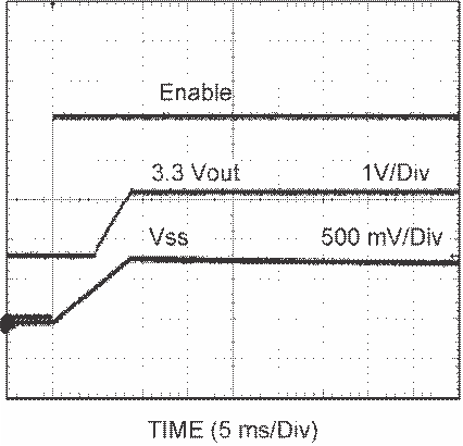 Figure 48. Prebiased Start-Up
7.3.6.1 Tracking Supply Divider Option
The tracking function allows the module to be connected as a slave supply to a primary voltage rail (often the 3.3-V system rail) where the slave module output voltage is lower than that of the master. Proper configuration allows the slave rail to power up coincident with the master rail such that the voltage difference between the rails during ramp-up is small (that is, < 0.15 V typical). The values for the tracking resistive divider must be selected such that the effect of the internal 50-µA current source is minimized. In most cases the ratio of the tracking divider resistors is the same as the ratio of the output voltage setting divider. Proper operation in tracking mode dictates the soft-start time of the slave rail be shorter than the master rail; a condition that is easy to satisfy because the CSS cap is replaced by RTKB. The tracking function is only supported for the power up interval of the master supply; once the SS/TRK rises past 0.795 V the input is no longer enabled and the 50-µA internal current source is switched off.
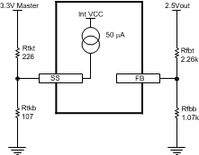 Figure 49. Tracking Option Input Detail
7.4 Device Functional Modes
7.4.1 Discontinuous Conduction and Continuous Conduction Modes
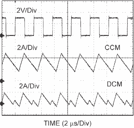
At light load the regulator will operate in discontinuous conduction mode (DCM). With load currents above the critical conduction point, it will operate in continuous conduction mode (CCM). When operating in DCM, inductor current is maintained to an average value equaling IOUT. In DCM the low-side switch will turn off when the inductor current falls to zero, this causes the inductor current to resonate. Although it is in DCM, the current is allowed to go slightly negative to charge the bootstrap capacitor.
In CCM, current flows through the inductor through the entire switching cycle and never falls to zero during the OFF-time.
Figure 50 is a comparison pair of waveforms showing both the CCM (upper) and DCM operating modes.
