SLVSBV7E June 2013 – February 2020 LMZ31707
PRODUCTION DATA.
- 1 Features
- 2 Applications
- 3 Description
- 4 Revision History
- 5 Specifications
- 6 Device Information
- 7 Typical Characteristics (PVIN = VIN = 12 V)
- 8 Typical Characteristics (PVIN = VIN = 5 V)
- 9 Typical Characteristics (PVIN = 3.3 V, VIN = 5 V)
-
10Application Information
- 10.1 Adjusting the Output Voltage
- 10.2 Capacitor Recommendations for the LMZ31707 Power Supply
- 10.3 Transient Response
- 10.4 Transient Waveforms
- 10.5 Application Schematics
- 10.6 Custom Design With WEBENCH® Tools
- 10.7 VIN and PVIN Input Voltage
- 10.8 3.3 V PVIN Operation
- 10.9 Power Good (PWRGD)
- 10.10 SYNC_OUT
- 10.11 Parallel Operation
- 10.12 Light Load Efficiency (LLE)
- 10.13 Power-Up Characteristics
- 10.14 Pre-Biased Start-up
- 10.15 Remote Sense
- 10.16 Thermal Shutdown
- 10.17 Output On/Off Inhibit (INH)
- 10.18 Slow Start (SS/TR)
- 10.19 Overcurrent Protection
- 10.20 Synchronization (CLK)
- 10.21 Sequencing (SS/TR)
- 10.22 Programmable Undervoltage Lockout (UVLO)
- 10.23 Layout Considerations
- 10.24 EMI
- 11Device and Documentation Support
- 12Mechanical, Packaging, and Orderable Information
Package Options
Mechanical Data (Package|Pins)
- RVQ|42
Thermal pad, mechanical data (Package|Pins)
Orderable Information
10.5 Application Schematics
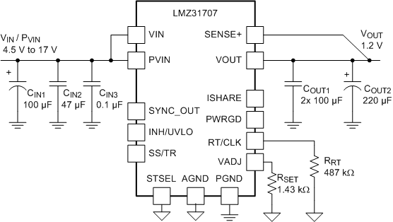
 Figure 20. Typical Schematic
PVIN = VIN = 4.5 V to 17 V, VOUT = 1.2 V
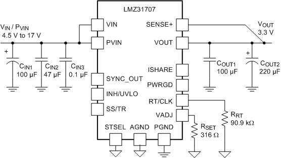
 Figure 21. Typical Schematic
PVIN = VIN = 4.5 V to 17 V, VOUT = 3.3 V
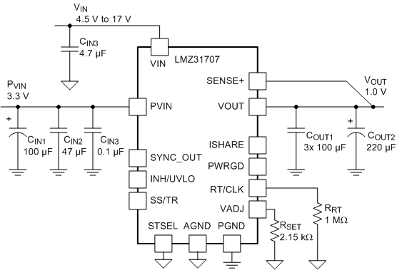
 Figure 22. Typical Schematic
PVIN = 3.3 V, VIN = 4.5 V to 17 V, VOUT = 1.0 V