SNVSB53C February   2018  – March 2023 LMZM23600

PRODUCTION DATA  

  1. Features
  2. Applications
  3. Description
  4. Revision History
  5. Device Comparison
  6. Pin Configuration and Functions
  7. Specifications
    1. 7.1 Absolute Maximum Ratings
    2. 7.2 ESD Ratings
    3. 7.3 Recommended Operating Conditions
    4. 7.4 Thermal Information
    5. 7.5 Electrical Characteristics
    6. 7.6 System Characteristics
    7. 7.7 Typical Characteristics
  8. Detailed Description
    1. 8.1 Overview
    2. 8.2 Functional Block Diagram
    3. 8.3 Feature Description
      1. 8.3.1 Control Scheme
      2. 8.3.2 Soft-Start Function
      3. 8.3.3 Enable and External UVLO Function
      4. 8.3.4 Current Limit
      5. 8.3.5 Hiccup Mode
      6. 8.3.6 Power Good (PGOOD) Function
      7. 8.3.7 MODE/SYNC Function
        1. 8.3.7.1 Forced PWM Mode
        2. 8.3.7.2 Auto PFM Mode
        3. 8.3.7.3 Dropout Mode
        4. 8.3.7.4 SYNC Operation
      8. 8.3.8 Thermal Protection
    4. 8.4 Device Functional Modes
      1. 8.4.1 Shutdown
      2. 8.4.2 FPWM Operation
      3. 8.4.3 Auto PFM Mode Operation
  9. Application and Implementation
    1. 9.1 Application Information
    2. 9.2 Typical Applications
      1. 9.2.1 Design Requirements
        1. 9.2.1.1 Maximum Input Voltage for VOUT < 2.5 V
      2. 9.2.2 Detailed Design Procedure
        1. 9.2.2.1 Custom Design With WEBENCH® Tools
        2. 9.2.2.2 Input Capacitor Selection
        3. 9.2.2.3 Output Capacitor Selection
        4. 9.2.2.4 Feedback Voltage Divider for Adjustable Output Voltage Versions
        5. 9.2.2.5 RPU - PGOOD Pullup Resistor
        6. 9.2.2.6 VIN Divider and Enable
      3. 9.2.3 Application Curves
        1. 9.2.3.1 VOUT = 5 V
        2. 9.2.3.2 VOUT = 3.3 V
        3. 9.2.3.3 VOUT = 12 V
        4. 9.2.3.4 VOUT = 15 V
        5. 9.2.3.5 VOUT = 2.5 V
        6. 9.2.3.6 VOUT = 1.2 V and VOUT = 1.8 V
        7. 9.2.3.7 VOUT = 5 V and 3.3 V Fixed Output Options
    3. 9.3 Best Design Practices
    4. 9.4 Power Supply Recommendations
      1. 9.4.1 Supply Voltage Range
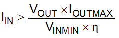
      2. 9.4.2 Supply Current Capability
      3. 9.4.3 Supply Input Connections
        1. 9.4.3.1 Voltage Drops
        2. 9.4.3.2 Stability
    5. 9.5 Layout
      1. 9.5.1 Layout Guidelines
        1. 9.5.1.1 Thermal Design
      2. 9.5.2 Layout Examples
  10. 10Device and Documentation Support
    1. 10.1 Device Support
      1. 10.1.1 Third-Party Products Disclaimer
      2. 10.1.2 Development Support
        1. 10.1.2.1 Custom Design With WEBENCH® Tools
    2. 10.2 Documentation Support
      1. 10.2.1 Related Documentation
    3. 10.3 Receiving Notification of Documentation Updates
    4. 10.4 Support Resources
    5. 10.5 Trademarks
    6. 10.6 Electrostatic Discharge Caution
    7. 10.7 Glossary
  11. 11Mechanical, Packaging, and Orderable Information
    1. 11.1 Tape and Reel Information

Package Options

Mechanical Data (Package|Pins)
Thermal pad, mechanical data (Package|Pins)
Orderable Information

Supply Current Capability

The input supply must be able to supply the required input current to the LMZM23600 converter. The required input current depends on the application's minimum input voltage, the required maximum output current, the output voltage, and the converter efficiency η for this condition.

Equation 4. GUID-E4841F63-7241-442E-B828-488C0FE453D3-low.gif

As an example, assuming that the adjustable output voltage version of the LMZM23600 is used for a 5-V, 0.5-A output converter design with 12-V minimum input voltage. The conversion efficiency for this condition is about 85%. The required input current from the supply is 0.49 A, so TI recommends an input power supply with ≥ 0.5 A current capability.