SNVSB11B June   2018  – May 2019 LMZM33606

PRODUCTION DATA.  

  1. Features
  2. Applications
    1.     Simplified Schematic
  3. Description
    1.     Minimum Solution Size
    2.     Typical Efficiency (Auto Mode)
  4. Revision History
  5. Pin Configuration and Functions
    1.     Pin Functions
  6. Specifications
    1. 6.1 Absolute Maximum Ratings
    2. 6.2 ESD Ratings
    3. 6.3 Recommended Operating Conditions
    4. 6.4 Thermal Information
    5. 6.5 Electrical Characteristics
    6. 6.6 Switching Characteristics
    7. 6.7 Typical Characteristics (VIN = 12 V)
    8. 6.8 Typical Characteristics (VIN = 24 V)
    9. 6.9 Typical Characteristics (VIN = 36 V)
  7. Detailed Description
    1. 7.1 Overview
    2. 7.2 Functional Block Diagram
    3. 7.3 Feature Description
      1. 7.3.1  Adjusting the Output Voltage
      2. 7.3.2  Input Capacitor Selection
      3. 7.3.3  Output Capacitor Selection
      4. 7.3.4  Transient Response
      5. 7.3.5  Feed-Forward Capacitor
      6. 7.3.6  Switching Frequency (RT)
      7. 7.3.7  Synchronization (SYNC/MODE)
      8. 7.3.8  Output Enable (EN)
      9. 7.3.9  Programmable System UVLO (EN)
      10. 7.3.10 Internal LDO and BIAS_SEL
      11. 7.3.11 Power Good (PGOOD) and Power Good Pull-Up (PGOOD_PU)
      12. 7.3.12 Mode Select (Auto or FPWM)
      13. 7.3.13 Soft Start and Voltage Tracking
      14. 7.3.14 Voltage Dropout
      15. 7.3.15 Overcurrent Protection (OCP)
      16. 7.3.16 Thermal Shutdown
    4. 7.4 Device Functional Modes
      1. 7.4.1 Active Mode
      2. 7.4.2 Auto Mode
      3. 7.4.3 FPWM Mode
      4. 7.4.4 Shutdown Mode
  8. Application and Implementation
    1. 8.1 Application Information
    2. 8.2 Typical Application
      1. 8.2.1 Design Requirements
      2. 8.2.2 Detailed Design Procedure
        1. 8.2.2.1 Output Voltage Setpoint
        2. 8.2.2.2 Setting the Switching Frequency
        3. 8.2.2.3 Input Capacitors
        4. 8.2.2.4 Output Capacitor Selection
        5. 8.2.2.5 Feed-Forward Capacitor (CFF)
        6. 8.2.2.6 Application Curves
  9. Power Supply Recommendations
  10. 10Layout
    1. 10.1 Layout Guidelines
    2. 10.2 Layout Example
    3. 10.3 Theta JA vs PCB Area
    4. 10.4 Package Specifications
    5. 10.5 EMI
      1. 10.5.1 EMI Plots
  11. 11Device and Documentation Support
    1. 11.1 Device Support
      1. 11.1.1 Third-Party Products Disclaimer
    2. 11.2 Receiving Notification of Documentation Updates
    3. 11.3 Community Resources
    4. 11.4 Trademarks
    5. 11.5 Electrostatic Discharge Caution
    6. 11.6 Glossary
  12. 12Mechanical, Packaging, and Orderable Information
    1. 12.1 Tape and Reel Information

Package Options

Refer to the PDF data sheet for device specific package drawings

Mechanical Data (Package|Pins)
  • RLX|41
Thermal pad, mechanical data (Package|Pins)
Orderable Information

EMI Plots

EMI plots were measured using the standard LMZM33606EVM with no input filter.
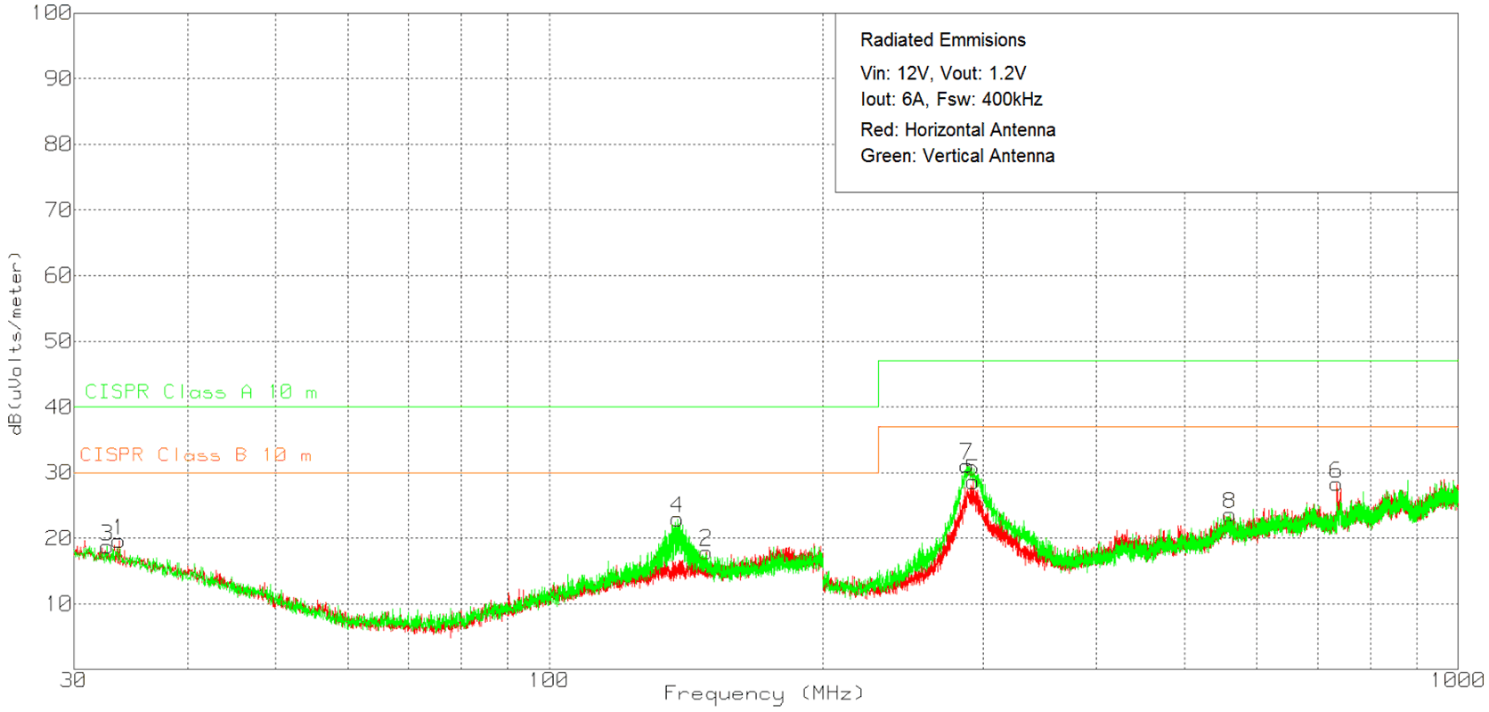
LMZM33606 EMI12V12V.gif
Figure 53. Radiated Emissions 12-V Input, 1.2-V Output, 6-A Load
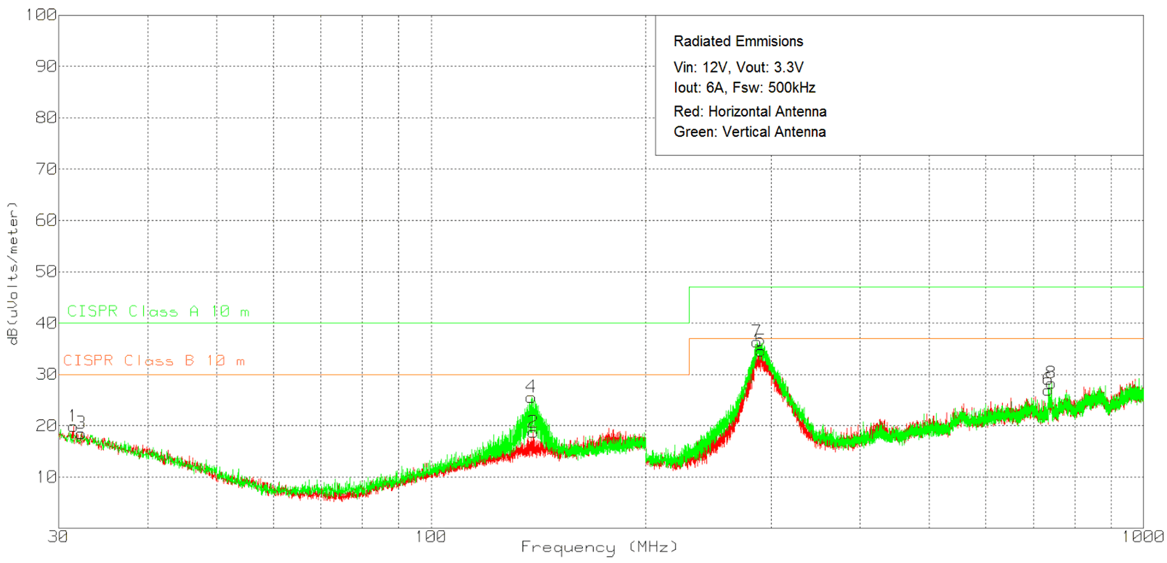
LMZM33606 EMI12V33V.gifFigure 54. Radiated Emissions 12-V Input, 3.3-V Output, 6-A Load
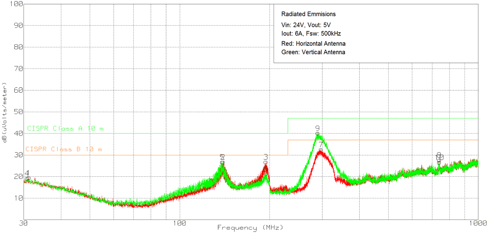
LMZM33606 EMI24V5V.gif
Figure 55. Radiated Emissions 24-V Input, 5-V Output, 6-A Load
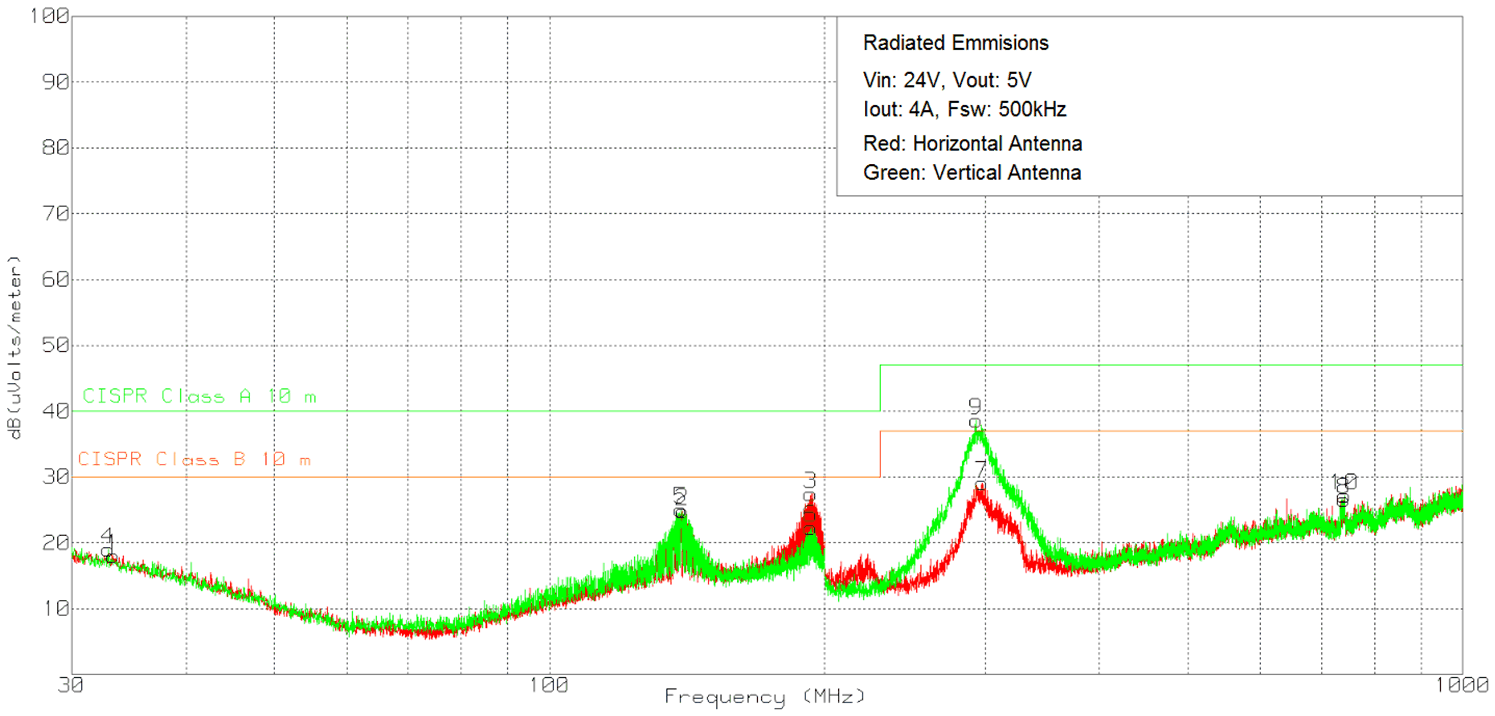
LMZM33606 EMI24V5V.gif
Figure 56. Radiated Emissions 24-V Input, 5-V Output, 4-A Load