SNVS096E June 1999 – July 2016 LP2954 , LP2954A
PRODUCTION DATA.
- 1 Features
- 2 Applications
- 3 Description
- 4 Revision History
- 5 Pin Configuration and Functions
- 6 Specifications
- 7 Detailed Description
- 8 Application and Implementation
- 9 Power Supply Recommendations
- 10Layout
- 11Device and Documentation Support
- 12Mechanical, Packaging, and Orderable Information
Package Options
Mechanical Data (Package|Pins)
Thermal pad, mechanical data (Package|Pins)
- KTT|3
Orderable Information
6 Specifications
6.1 Absolute Maximum Ratings
over operating free-air temperature range (unless otherwise noted)(2)(1)| MIN | MAX | UNIT | ||
|---|---|---|---|---|
| Input supply voltage | –20 | 30 | V | |
| Power dissipation(2) | Internally Limited | |||
| Storage temperature, Tstg | –65 | 150 | °C | |
(1) If Military/Aerospace specified devices are required, please contact the Texas Instruments Sales Office/Distributors for availability and specifications.
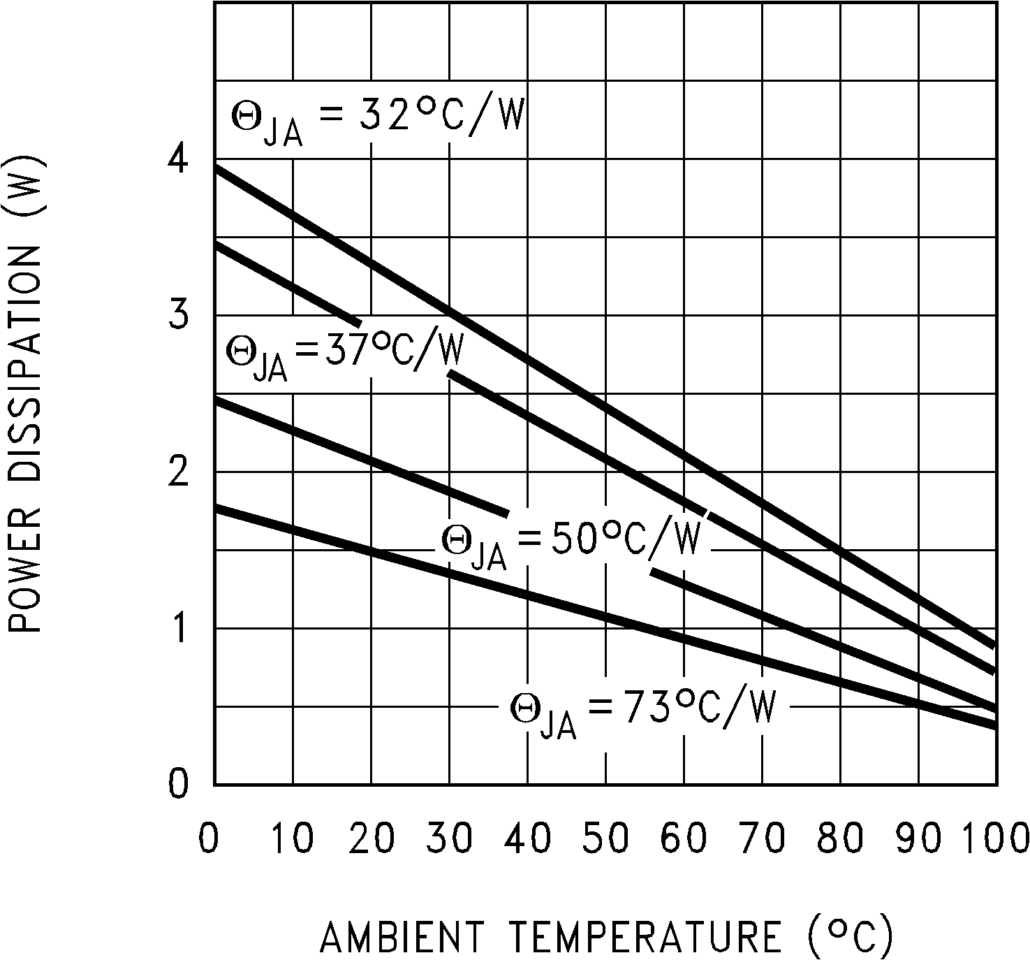
(2) At elevated temperatures, device power dissipation must be derated based on package thermal resistance and heat sink values (if a heat sink is used). If power dissipation causes the junction temperature to exceed specified limits, the device goes into thermal shutdown.
6.2 ESD Ratings
| VALUE | UNIT | |||
|---|---|---|---|---|
| V(ESD) | Electrostatic discharge | Human-body model (HBM), per ANSI/ESDA/JEDEC JS-001(1) | ±2000 | V |
(1) JEDEC document JEP155 states that 500-V HBM allows safe manufacturing with a standard ESD control process.
6.3 Recommended Operating Conditions
over operating free-air temperature range (unless otherwise noted)| MIN | NOM | MAX | UNIT | ||
|---|---|---|---|---|---|
| Operating junction temperature | –40 | 125 | °C | ||
6.4 Thermal Information
| THERMAL METRIC(1) | LP2954, LP2954A | UNIT | |||
|---|---|---|---|---|---|
| KTT (DDPAK/TO-263) | NDE (TO-220) | D (SOIC) | |||
| 3 PINS | 3 PINS | 8 PINS | |||
| RθJA(2) | Junction-to-ambient thermal resistance, High-K | 44.3 | 80.3(3) | 105.0 | °C/W |
| RθJC(top) | Junction-to-case (top) thermal resistance | 44.8 | 38.6 | 47.3 | °C/W |
| RθJB | Junction-to-board thermal resistance | 23.8 | 73.1 | 45.8 | °C/W |
| ψJT | Junction-to-top characterization parameter | 10.6 | 13.5 | 6.2 | °C/W |
| ψJB | Junction-to-board characterization parameter | 22.7 | 73.1 | 45.2 | °C/W |
| RθJC(bot) | Junction-to-case (bottom) thermal resistance | 1.0 | 0.9 | — | °C/W |
(1) For more information about traditional and new thermal metrics, see Semiconductor and IC Package Thermal Metrics.
(2) Thermal resistance value RθJA is based on the EIA/JEDEC High-K printed circuit board defined by JESD51-7 - High Effective Thermal Conductivity Test Board for Leaded Surface Mount Packages.
(3) The TO-220 (NDE) package is vertically mounted in center of JEDEC High-K test board (JESD 51-7) with no additional heat sink. This is a through-hole package; this is NOT a surface mount package.
6.5 Electrical Characteristics
Limits are specified by production testing or correlation techniques using standard Statistical Quality Control (SQC) methods. Unless otherwise noted: TJ = 25°C, VIN = 6 V, IL = 1 mA, CL = 2.2 μF| PARAMETER | TEST CONDITIONS | LP2954AI | LP2954I | UNIT | |||||
|---|---|---|---|---|---|---|---|---|---|
| MIN | TYP | MAX | MIN | TYP | MAX | ||||
| VO | Output voltage(1) | 4.975 | 5 | 5.025 | 4.95 | 5 | 5.05 | V | |
| −40°C to 125°C | 4.94 | 5.06 | 4.9 | 5.1 | |||||
| 1 mA ≤ IL ≤ 250 mA | 5 | 5 | |||||||
| 1 mA ≤ IL ≤ 250 mA −40°C to 125°C |
4.93 | 5.07 | 4.88 | 5.12 | |||||
| ΔVO/ΔT | Output voltage temperature coefficient | See(2), –40°C ≤ TJ ≤ 125°C | 20 | 100 | 20 | 150 | ppm/°C | ||
| ΔVO/VO | Line regulation | VIN = 6 V to 30 V | 0.03% | 0.1% | 0.03% | 0.2% | |||
| VIN = 6 V to 30 V –40°C ≤ TJ ≤ 125°C |
0.2% | 0.3% | |||||||
| ΔVO/VO | Load regulation | IL = 1 to 250 mA IL = 0.1 to 1 mA(3) |
0.04% | 0.16% | 0.04% | 0.2% | |||
| IL = 1 to 250 mA IL = 0.1 to 1 mA –40°C ≤ TJ ≤ 125°C |
0.2% | 0.3% | |||||||
| VIN – VO | Dropout voltage(4) | IL = 1 mA | 60 | 100 | 60 | 100 | mV | ||
| IL = 1 mA –40°C ≤ TJ ≤ 125°C |
150 | 150 | |||||||
| IL = 50 mA | 240 | 300 | 240 | 300 | |||||
| IL = 50 mA, –40°C ≤ TJ ≤ 125°C |
420 | 420 | |||||||
| IL = 100 mA | 310 | 400 | 310 | 400 | |||||
| IL = 100 mA –40°C ≤ TJ ≤ 125°C |
520 | 520 | |||||||
| IL = 250 mA | 470 | 600 | 470 | 600 | |||||
| IL = 250 mA –40°C ≤ TJ ≤ 125°C |
800 | 800 | |||||||
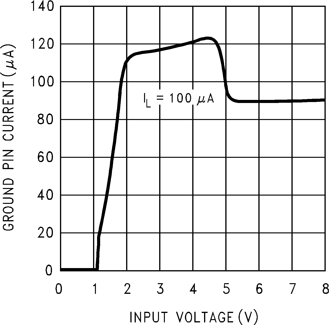
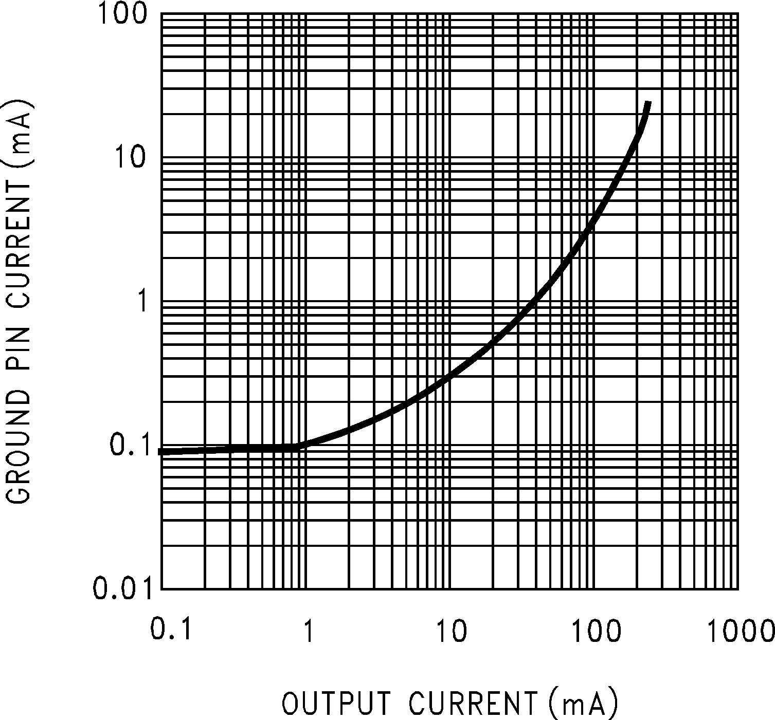
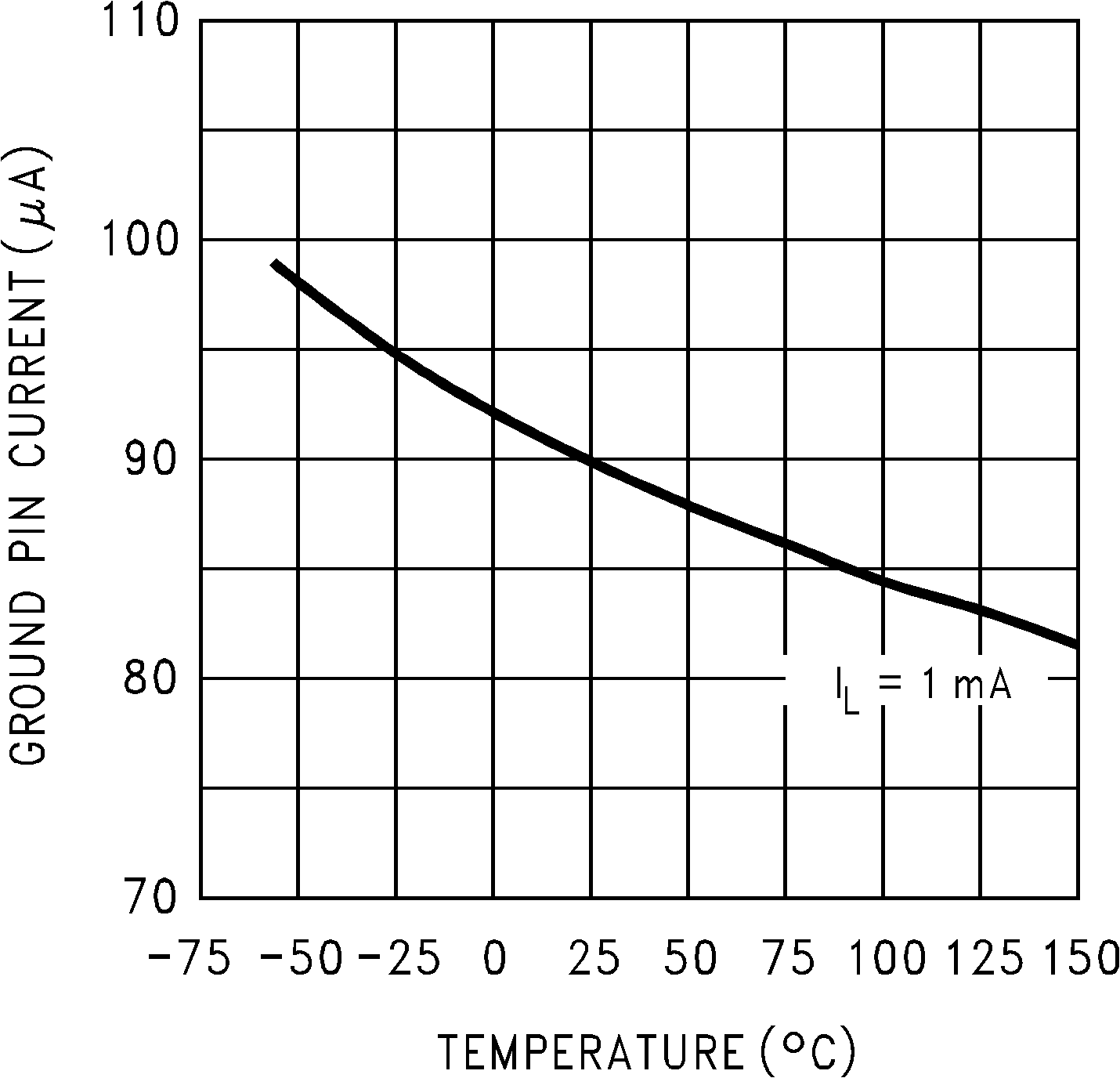
| IGND | Ground pin current(5) | IL = 1 mA | 90 | 150 | 90 | 150 | µA | ||
| IL = 1 mA –40°C ≤ TJ ≤ 125°C |
180 | 180 | |||||||
| IL = 50 mA | 1.1 | 2 | 1.1 | 2 | mA | ||||
| IL = 50 mA –40°C ≤ TJ ≤ 125°C |
2.5 | 2.5 | |||||||
| IL = 100 mA | 4.5 | 6 | 4.5 | 6 | |||||
| IL = 100 mA –40°C ≤ TJ ≤ 125°C |
8 | 8 | |||||||
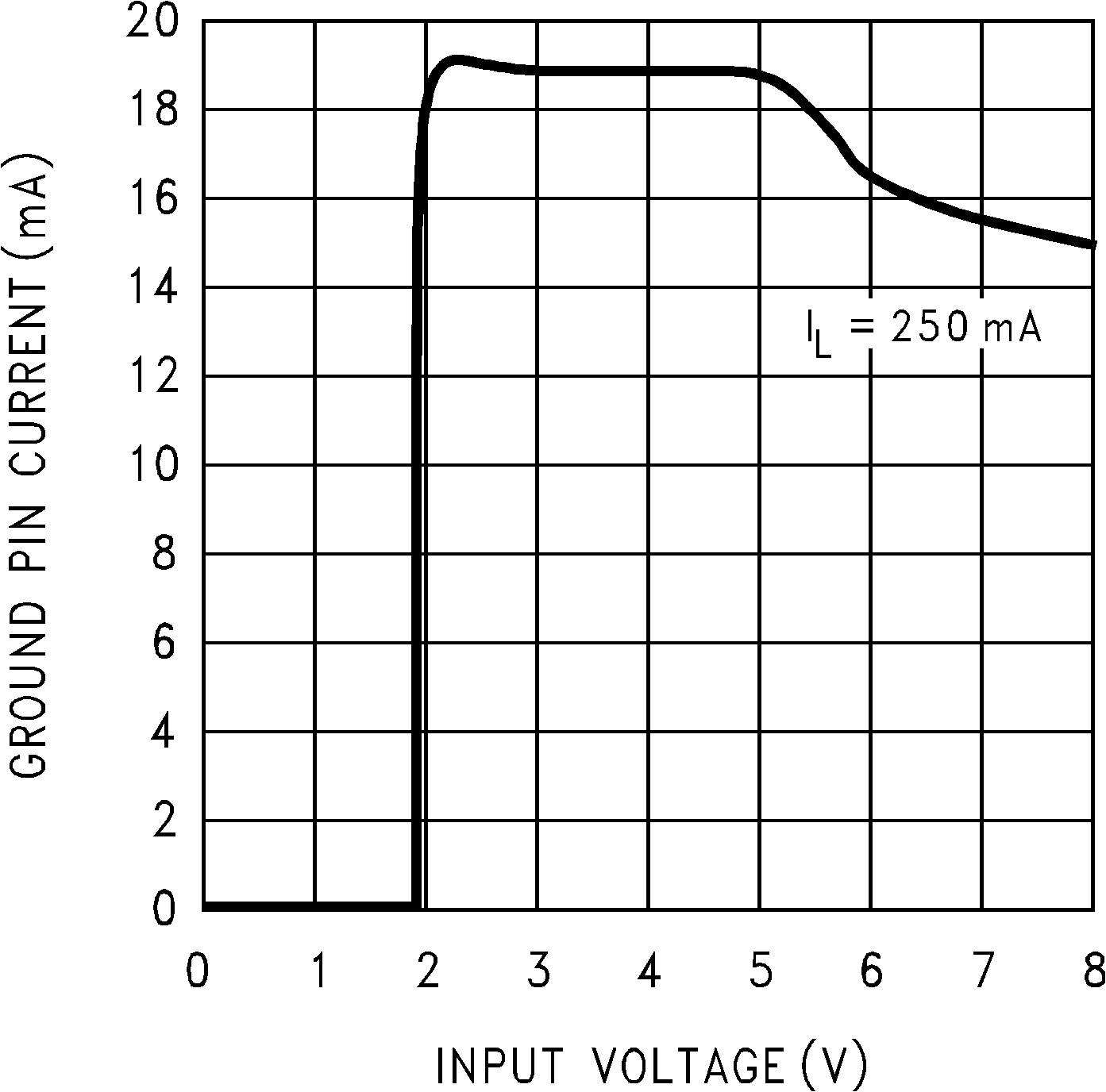
| IL = 250 mA | 21 | 28 | 21 | 28 | |||||
| IL = 250 mA –40°C ≤ TJ ≤ 125°C |
33 | 33 | |||||||
| IGND | Ground pin current at dropout(5) | VIN = 4.5 V | 120 | 170 | 120 | 170 | µA | ||
| VIN = 4.5 V –40°C ≤ TJ ≤ 125°C |
210 | 210 | |||||||
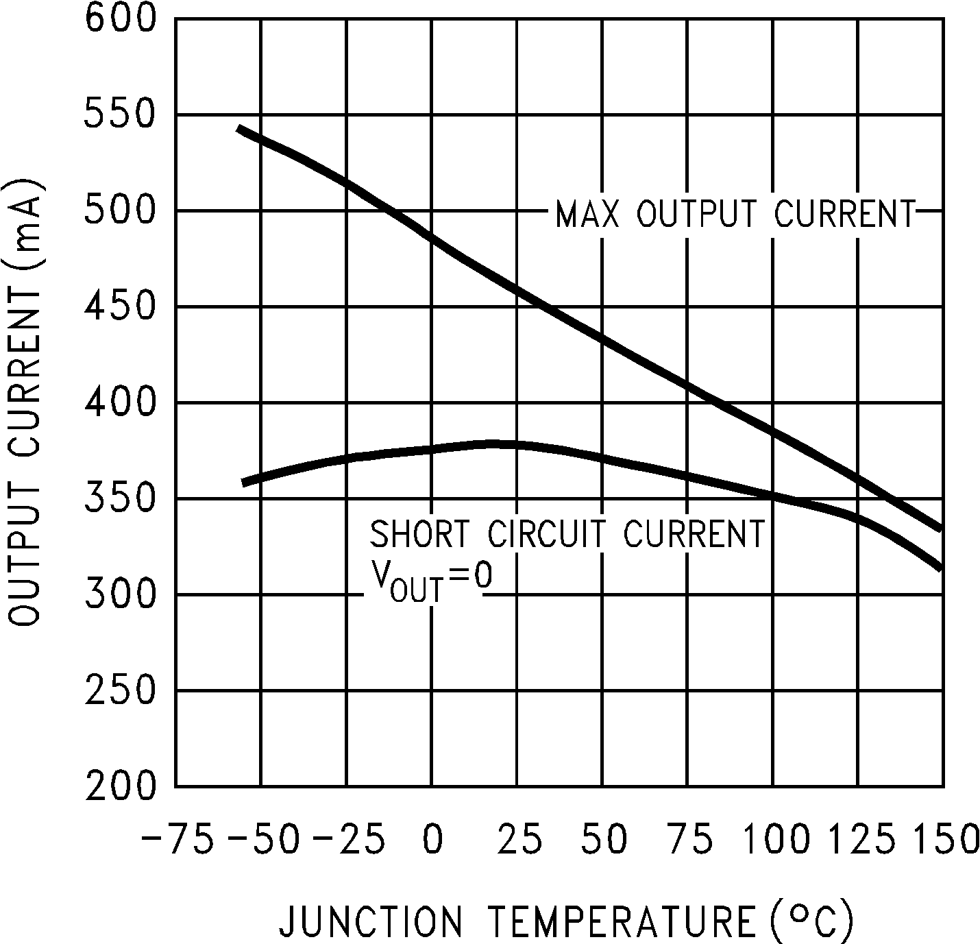
| ILIMIT | Current limit | VO = 0 V | 380 | 500 | 380 | 500 | mA | ||
| VO = 0 V –40°C ≤ TJ ≤ 125°C |
530 | 530 | |||||||
| ΔVO/ΔPD | Thermal regulation | See(6) | 0.05 | 0.2 | 0.05 | 0.2 | %/W | ||
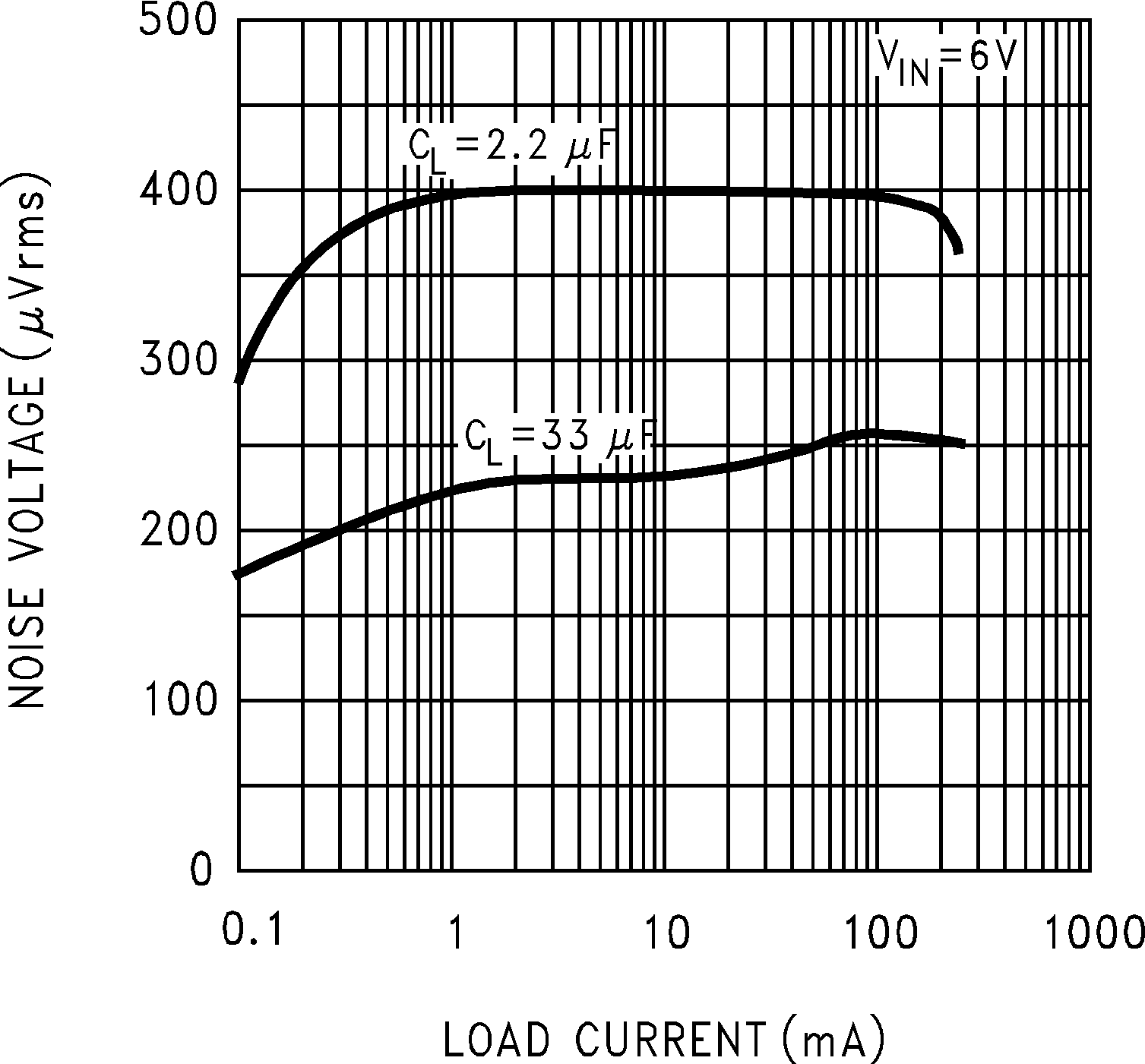
| en | Output noise 10 Hz to 100 kHz |
IL = 100 mA, CL = 2.2 µF | 400 | 400 | μVRMS | ||||
| IL = 100 mA, CL = 33 µF | 260 | 260 | |||||||
| IL = 100 mA, CL = 33 µF(7) | 80 | 80 | |||||||
| ADDITIONAL SPECIFICATIONS FOR THE ADJUSTABLE DEVICE (LP2954AIM and LP2954IM) | |||||||||
| VREF | Reference voltage | See(8) | 1.215 | 1.23 | 1.245 | 1.205 | 1.23 | 1.255 | V |
| See(8)
–40°C ≤ TJ ≤ 125°C |
1.205 | 1.255 | 1.19 | 1.27 | |||||
| ΔVREF/ VREF |
Reference voltage line regulation | VIN= 2.5 V to VO(NOM) + 1 V | 0.03% | 0.1% | 0.03% | 0.2% | |||
| VIN= 2.5 V to VO(NOM) +1 V to 30 V(9)(8)–40°C ≤ TJ ≤ 125°C | 0.2% | 0.4% | |||||||
| ΔVREF/ΔT | Reference voltage temperature coefficient | See(2)
–40°C ≤ TJ ≤ 125°C |
20 | ppm/°C | |||||
| IB(FB) | Feedback pin bias current | 20 | 40 | 20 | 40 | nA | |||
| –40°C ≤ TJ ≤ 125°C | 60 | 60 | |||||||
| IGND | Ground pin current at shutdown(5) | VSHUTDOWN ≤ 1.1 V | 105 | 140 | 105 | 140 | μA | ||
| IO(SINK) | Output OFF pulldown current | See(10) | 30 | 30 | mA | ||||
| See(10)
–40°C ≤ TJ ≤ 125°C |
20 | 20 | |||||||
| DROPOUT DETECTION COMPARATOR | |||||||||
| IOH | Output HIGH leakage current | VOH = 30 V | 0.01 | 1 | 0.01 | 1 | µA | ||
| VOH = 30 V, –40°C ≤ TJ ≤ 125°C | 2 | 2 | |||||||
| VOL | Output LOW voltage | VIN = VO(NOM) − 0.5 V IO(COMP) = 400 μA –40°C ≤ TJ ≤ 125°C |
150 | 250 | 150 | 250 | mV | ||
| 400 | 400 | ||||||||
| VTHR(MAX) | Upper threshold voltage | See(11) | –80 | –60 | –35 | –80 | –60 | –35 | mV |
| See(11)
–40°C ≤ TJ ≤ 125°C |
–95 | –25 | –95 | –25 | |||||
| VTHR(MIN) | Lower threshold voltage | See(11) | –110 | –85 | –55 | –110 | –85 | –55 | mV |
| See(11)
–40°C ≤ TJ ≤ 125°C |
–160 | –40 | –160 | –40 | |||||
| HYST | Hysteresis | See(11) | 15 | 15 | mV | ||||
| SHUTDOWN INPUT | |||||||||
| VOS | Input offset voltage | (Referred to VREF) | −7.5 | ±3 | 7.5 | −7.5 | ±3 | 7.5 | mV |
| (Referred to VREF), –40°C ≤ TJ ≤ 125°C | –10 | 10 | –10 | 10 | |||||
| HYST | Hysteresis | 6 | 6 | mV | |||||
| IB | Input bias current | VIN(SHUTDOWN) = 0 V to 5 V | –30 | 10 | 30 | –30 | 10 | 30 | nA |
| VIN(SHUTDOWN) = 0 V to 5 V, –40°C ≤ TJ ≤ 125°C |
–50 | 50 | –50 | 50 | |||||
(1) When used in dual-supply systems where the regulator load is returned to a negative supply, the output voltage must be diode-clamped to ground.
(2) Output voltage temperature coefficient is defined as the worst-case voltage change divided by the total temperature range.
(3) Regulation is measured at constant junction temperature using low duty cycle pulse testing. Parts are tested separately for load regulation in the load ranges 0.1 mA to 1 mA and 1 mAto 250 mA. Changes in output voltage due to heating effects are covered by the thermal regulation specification.
(4) Dropout voltage is defined as the input-to-output differential at which the output voltage drops 100 mV below the value measured with a 1-V differential.
(5) GND pin current is the regulator quiescent current. The total current drawn from the source is the sum of the load current plus the GND pin current.
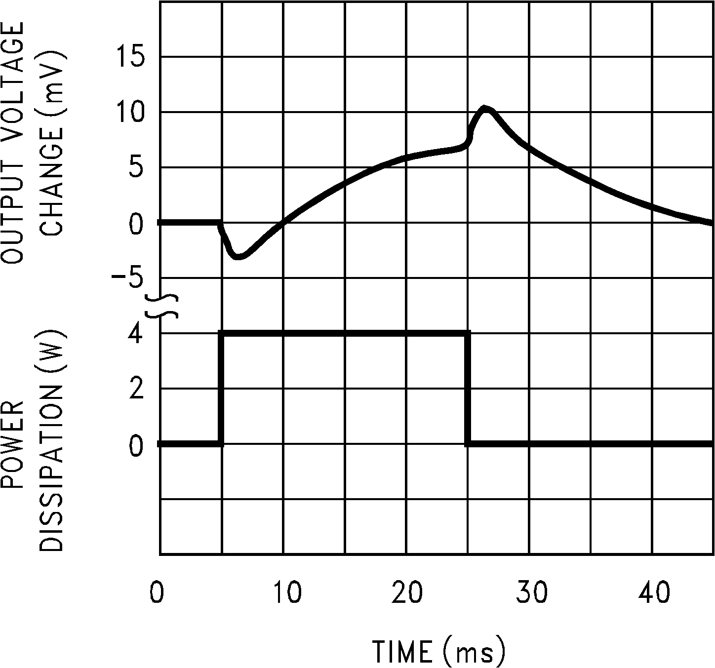
(6) Thermal regulation is defined as the change in output voltage at a time T after a change in power dissipation is applied, excluding load or line regulation effects. Specifications are for 200-mA load pulse at VIN = 20 V (3-W pulse) for T = 10 ms.
(7) Connect a 0.1-μF capacitor from the OUT pin to the FEEDBACK pin.
(8) VREF ≤ VOUT ≤ (VIN − 1 V), 2.3 V ≤ VIN ≤ 30 V, 100 μA ≤ IL≤ 250 mA.
(9) Two separate tests are performed, one covering VIN = 2.5 V to VO(NOM) + 1 V and the other test for VIN = 2.5 V to VO(NOM) + 1 V to 30 V.
(10) VSHUTDOWN ≤ 1.1 V, VOUT = VO(NOM).
(11) Comparator thresholds are expressed in terms of a voltage differential at the FEEDBACK pin below the nominal reference voltage measured at VIN = VO(NOM) + 1 V. To express these thresholds in terms of output voltage change, multiply by the error amplifier gain, which is VOUT/VREF = (R1 + R2 ) / R2.
6.6 Typical Characteristics
