SNVS539H November 2007 – September 2015 LP38500-ADJ , LP38502-ADJ
PRODUCTION DATA.
- 1 Features
- 2 Applications
- 3 Description
- 4 Revision History
- 5 Pin Configurations and Functions
- 6 Specifications
- 7 Detailed Description
- 8 Application and Implementation
- 9 Power Supply Recommendations
- 10Layout
- 11Device and Documentation Support
- 12Mechanical, Packaging, and Orderable Information
Package Options
Mechanical Data (Package|Pins)
Thermal pad, mechanical data (Package|Pins)
- KTT|5
Orderable Information
10 Layout
10.1 Layout Guidelines
10.1.1 Printed Circuit Board Layout
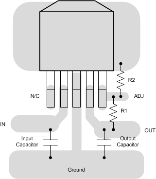
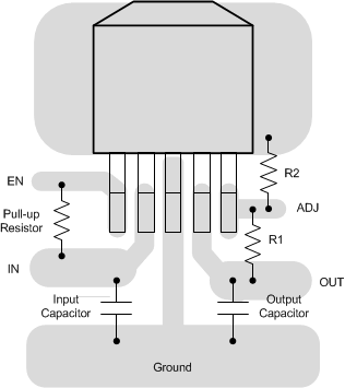
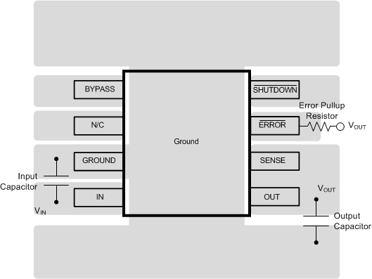
Good layout practices will minimize voltage error and prevent instability which can result from ground loops. The input and output capacitors should be directly connected to the device pins with short traces that have no other current flowing in them (Kelvin connect).
The best way to do this is to place the capacitors very near the device and make connections directly to the device pins via short traces on the top layer of the PCB. The regulator’s ground pin should be connected through vias to the internal or backside ground plane so that the regulator has a single point ground.
The external resistors which set the output voltage must also be located very near the device with all connections directly tied via short traces to the pins of the device (Kelvin connect). Do not connect the resistive divider to the load point or DC error will be induced.
10.2 Layout Examples
 Figure 22. LP38500-ADJ TO-263 Layout (LP38500)
 Figure 23. LP38502-ADJ TO-263 Layout
 Figure 24. LP3850x WSON Layout
10.2.1 Heatsinking WSON Package
The junction-to-ambient thermal resistance for the WSON package is dependent on how much PCB copper is present to conduct heat away from the device. The LP38502SD-ADJ evaluation board (980600046-100) was tested and gave a result of about 52.5°C/W with a power dissipation of 1 W and no external airflow. This evaluation board is a two layer board using two ounce copper, and the copper area on topside for heatsinking is approximately two square inches. Multiple vias under the DAP also thermally connect to the backside layer which has about three square inches of copper dedicated to heatsinking.
With four thermal vias directly under the DAP to the first copper plane, the modeling predicts a RθJA of 52.5°C/W.
Adding a dog-bone copper area with four additional thermal vias in the dog-bone area to the first copper plane can improve RθJA to 45°C/W.
See Application Note AN-1520 A Guide to Board Layout for Best Thermal Resistance for Exposed Packages (SNVA183) for additional thermal considerations for printed circuit board layouts.