SNVS322M December 2004 – December 2015 LP38690 , LP38692
PRODUCTION DATA.
- 1 Features
- 2 Applications
- 3 Description
- 4 Revision History
- 5 Pin Configuration and Functions
- 6 Specifications
- 7 Detailed Description
- 8 Application and Implementation
- 9 Power Supply Recommendations
- 10Layout
- 11Device and Documentation Support
- 12Mechanical, Packaging, and Orderable Information
Package Options
Mechanical Data (Package|Pins)
Thermal pad, mechanical data (Package|Pins)
Orderable Information
10 Layout
10.1 PCB Layout
The dynamic performance of the LP38690 and LP38692 devices is dependent on the layout of the PCB. PCB layout practices that are adequate for typical LDOs may degrade the load regulation, PSRR, noise, or transient performance of the LP38690 or LP38692.
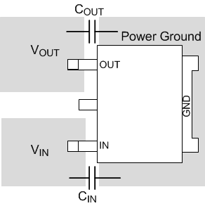
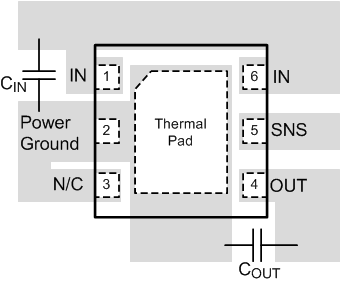
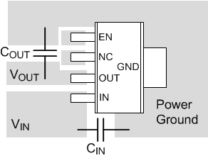
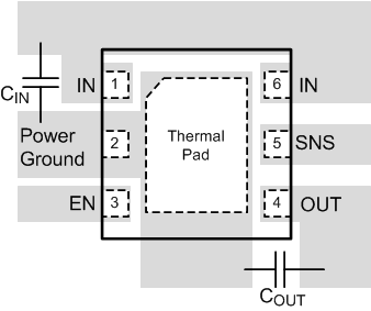
Best performance is achieved by placing CIN and COUT on the same side of the PCB as the LP38690 or LP38692, and as close to the package as is practical. The ground connections for CIN and COUT must be back to the LP38690 or LP38692 GND pin using as wide and short a copper trace as is practical.
Connections using long trace lengths, narrow trace widths, or connections through vias must be avoided. These add parasitic inductances and resistance that result in inferior performance especially during transient conditions.
A ground plane, either on the opposite side of a two-layer PCB, or embedded in a multi-layer PCB, is strongly recommended. This ground plane serves two purposes:
- Provides a circuit reference plane to assure accuracy, and
- provides a thermal plane to remove heat from the LP38690 or LP38692 WSON package through thermal vias under the package DAP.
10.2 Layout Examples
 Figure 35. LP38690 TO-252 Package
 Figure 37. LP38690 WSON Package
 Figure 36. LP38692 SOT-223 Package
 Figure 38. LP38692 WSON Package
10.3 WSON Mounting
The NGG0006A (No Pullback) 6-Lead WSON package requires specific mounting techniques which are detailed in the TI Application Report AN-1187 Leadless Leadframe Package (LLP) (SNOA401). Referring to the section PCB Design Recommendations (Page 5), it should be noted that the pad style which should be used with the WSON package is the NSMD (non-solder mask defined) type. Additionally, it is recommended the PCB terminal pads to be 0.2 mm longer than the package pads to create a solder fillet to improve reliability and inspection.
The input current is split between two IN pins, 1 and 6. The two IN pins must be connected together to ensure that the device can meet all specifications at the rated current.
The thermal dissipation of the WSON package is directly related to the printed circuit board construction and the amount of additional copper area connected to the DAP.
The DAP (exposed pad) on the bottom of the WSON package is connected to the die substrate with a conductive die attach adhesive. The DAP has no direct electrical (wire) connection to any of the pins. There is a parasitic PN junction between the die substrate and the device ground. As such, it is strongly recommend that the DAP be connected directly to the ground at device lead 2 (such as GND). Alternately, but not recommended, the DAP may be left floating (that is, no electrical connection). The DAP must not be connected to any potential other than ground.
10.4 RFI/EMI Susceptibility
Radio frequency interference (RFI) and electromagnetic interference (EMI) can degrade any integrated circuit’s performance because of the small dimensions of the geometries inside the device. In applications where circuit sources are present which generate signals with significant high frequency energy content (> 1 MHz), care must be taken to ensure that this does not affect the device regulator.
If RFI/EMI noise is present on the input side of the regulator (such as applications where the input source comes from the output of a switching regulator), good ceramic bypass capacitors must be used at the IN pin of the device.
If a load is connected to the device output which switches at high speed (such as a clock), the high-frequency current pulses required by the load must be supplied by the capacitors on the device output. Since the bandwidth of the regulator loop is less than 100 kHz, the control circuitry cannot respond to load changes above that frequency. This means the effective output impedance of the device at frequencies above 100 kHz is determined only by the output capacitors.
In applications where the load is switching at high speed, the output of the device may need RF isolation from the load. It is recommended that some inductance be placed between the output capacitor and the load, and good RF bypass capacitors be placed directly across the load.
PCB layout is also critical in high noise environments, since RFI/EMI is easily radiated directly into PC traces. Noisy circuitry should be isolated from clean circuits where possible, and grounded through a separate path. At MHz frequencies, ground planes begin to look inductive and RFI/ EMI can cause ground bounce across the ground plane. In multi-layer PCB applications, care should be taken in layout so that noisy power and ground planes do not radiate directly into adjacent layers which carry analog power and ground.
10.5 Output Noise
Noise is specified in two ways: Spot Noise or Output Noise Density is the RMS sum of all noise sources, measured at the regulator output, at a specific frequency (measured with a 1-Hz bandwidth). This type of noise is usually plotted on a curve as a function of frequency. Total Output Noise or Broad-Band Noise is the RMS sum of spot noise over a specified bandwidth, usually several decades of frequencies.
Attention should be paid to the units of measurement. Spot noise is measured in units µV/√Hz or nV/√Hz and total output noise is measured in µVRMS
The primary source of noise in low-dropout regulators is the internal reference. Noise can be reduced in two ways: by increasing the transistor area or by increasing the current drawn by the internal reference. Increasing the area decreases the chance of fitting the die into a smaller package. Increasing the current drawn by the internal reference increases the total supply current (GND pin current).