SNVS227H February 2003 – January 2015 LP3872 , LP3875
PRODUCTION DATA.
- 1 Features
- 2 Applications
- 3 Description
- 4 Revision History
- 5 Pin Configuration and Functions
- 6 Specifications
- 7 Detailed Description
-
8 Application and Implementation
- 8.1 Application Information
- 8.2
Typical Application
- 8.2.1 Design Requirements
- 8.2.2 Detailed Design Procedure
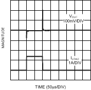
- 8.2.3 Application Curves
- 9 Power Supply Recommendations
- 10Layout
- 11Device and Documentation Support
- 12Mechanical, Packaging, and Orderable Information
Package Options
Mechanical Data (Package|Pins)
Thermal pad, mechanical data (Package|Pins)
- KTT|5
Orderable Information
8 Application and Implementation
NOTE
Information in the following applications sections is not part of the TI component specification, and TI does not warrant its accuracy or completeness. TI’s customers are responsible for determining suitability of components for their purposes. Customers should validate and test their design implementation to confirm system functionality.
8.1 Application Information
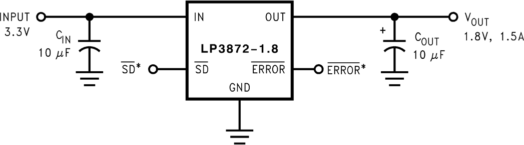
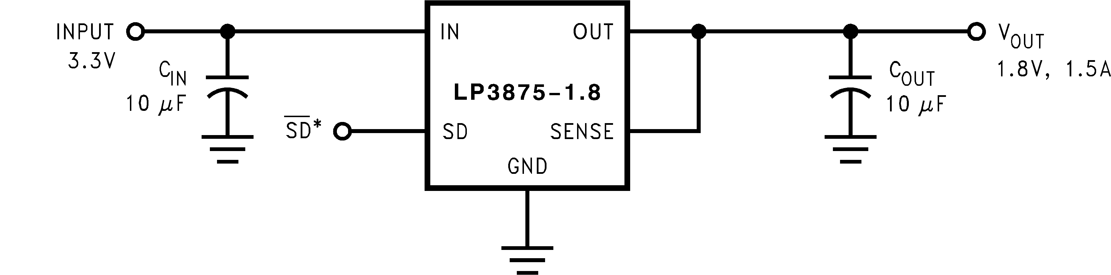
The LP387x devices are linear regulators designed to provide high load current of up to 1.5 A, low dropout voltage, and low quiescent current in shutdown mode. Figure 12 and Figure 13 show the typical application circuit for these devices.
8.1.1 Dropout Voltage
The dropout voltage of a regulator is defined as the minimum input-to-output differential required to stay within 2% of the nominal output voltage. For CMOS LDOs, the dropout voltage is the product of the load current and the Rds(on) of the internal MOSFET.
8.1.2 Reverse Current Path
The internal MOSFET in LP3872 and LP3875 has an inherent parasitic diode. During normal operation, the input voltage is higher than the output voltage and the parasitic diode is reverse biased. However, if the output is pulled above the input in an application, then current flows from the output to the input as the parasitic diode gets forward biased. The output can be pulled above the input as long as the current in the parasitic diode is limited to 200-mA continuous and 1-A peak.
8.2 Typical Application
8.2.1 Design Requirements
Table 1. Design Parameters
| DESIGN PARAMETER | EXAMPLE VALUE |
|---|---|
| Input voltage range | 2.5 V to 7 V |
| Output voltage | 1.8 V |
| Output current | 1.5 A |
| Output capacitor | 10 µF |
| Input capacitor | 10 µF |
| Output capacitor ESR range | 100 mΩ to 4 Ω |
8.2.2 Detailed Design Procedure
8.2.2.1 Power Dissipation and Device Operation
The permissible power dissipation for any package is a measure of the capability of the device to pass heat from the power source, the junctions of the IC, to the ultimate heat sink, the ambient environment. Thus, the power dissipation depends on the ambient temperature and the thermal resistance across the various interfaces between the die junction and ambient air.
The maximum allowable power dissipation for the device in a given package can be calculated using Equation 1:
The actual power being dissipated in the device can be represented by Equation 2:
Equation 1 and Equation 2 establish the relationship between the maximum power dissipation allowed due to thermal consideration, the voltage drop across the device, and the continuous current capability of the device. These two equations should be used to determine the optimum operating conditions for the device in the application.
In applications where lower power dissipation (PD) and/or excellent package thermal resistance (RθJA) is present, the maximum ambient temperature (TA-MAX) may be increased.
In applications where high power dissipation and/or poor package thermal resistance is present, the maximum ambient temperature (TA-MAX) may have to be derated. TA-MAX is dependent on the maximum operating junction temperature (TJ-MAX-OP = 125°C), the maximum allowable power dissipation in the device package in the application (PD-MAX), and the junction-to ambient thermal resistance of the part/package in the application (RθJA), as given by Equation 3:
Alternately, if TA-MAX can not be derated, the PD value must be reduced. This can be accomplished by reducing VIN in the VIN – VOUT term as long as the minimum VIN is met, or by reducing the IOUT term, or by some combination of the two.
8.2.2.2 External Capacitors
Like any low-dropout regulator, external capacitors are required to assure stability. These capacitors must be correctly selected for proper performance.
- Input Capacitor: An input capacitor of at least 10 µF is required. Ceramic, tantalum, or Electrolytic capacitors may be used, and capacitance may be increased without limit.
- Output Capacitor: An output capacitor is required for loop stability. It must be located less than 1 cm from the device and connected directly to the output and ground pins using traces which have no other currents flowing through them (see Layout section).
The minimum value of output capacitance that can be used for stable full-load operation is 10 µF, but it may be increased without limit. The output capacitor must have an equivalent series resistance (ESR) value as shown in Figure 14. Tantalum capacitors are recommended for the output capacitor.
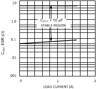 Figure 14. ESR Curve
8.2.2.3 Selecting a Capacitor
Capacitance tolerance and variation with temperature must be considered when selecting a capacitor so that the minimum required amount of capacitance is provided over the full operating temperature range. In general, a good tantalum capacitor will show very little capacitance variation with temperature, but a ceramic may not be as good (depending on dielectric type). Aluminum electrolytics also typically have large temperature variation of capacitance value.
Equally important to consider is how ESR of a capacitor changes with temperature: this is not an issue with ceramics, as their ESR is extremely low. However, it is very important in tantalum and aluminum electrolytic capacitors. Both show increasing ESR at colder temperatures, but the increase in aluminum electrolytic capacitors is so severe they may not be feasible for some applications (see Capacitor Characteristics).
8.2.2.4 Capacitor Characteristics
8.2.2.4.1 Ceramic
For values of capacitance in the 10-µF to 100-µF range, ceramics are usually larger and more costly than tantalums but give superior AC performance for bypassing high frequency noise because of very low ESR (typically less than 10 mΩ). However, some dielectric types do not have good capacitance characteristics as a function of voltage and temperature.
Z5U and Y5V dielectric ceramics have capacitance that drops severely with applied voltage. A typical Z5U or Y5V capacitor can lose 60% of its rated capacitance with half of the rated voltage applied to it. The Z5U and Y5V also exhibit a severe temperature effect, losing more than 50% of nominal capacitance at high and low limits of the temperature range.
X7R and X5R dielectric ceramic capacitors are strongly recommended if ceramics are used, as they typically maintain a capacitance range within ±20% of nominal over full operating ratings of temperature and voltage. Of course, they are typically larger and more costly than Z5U/Y5U types for a given voltage and capacitance.
8.2.2.4.2 Tantalum
Solid tantalum capacitors are recommended for use on the output because their typical ESR is very close to the ideal value required for loop compensation. They also work well as input capacitors if selected to meet the ESR requirements previously listed.
Tantalums also have good temperature stability: a good quality tantalum will typically show a capacitance value that varies less than 10-15% across the full temperature range of −40°C to 125°C. ESR will vary only about 2X going from the high to low temperature limits.
The increasing ESR at lower temperatures can cause oscillations when marginal quality capacitors are used (if the ESR of the capacitor is near the upper limit of the stability range at room temperature).
8.2.2.4.3 Aluminum
This capacitor type offers the most capacitance for the money. The disadvantages are that they are larger in physical size, not widely available in surface mount, and have poor AC performance (especially at higher frequencies) due to higher ESR and equivalent series inductance (ESL).
Compared by size, the ESR of an aluminum electrolytic is higher than either tantalum or ceramic, and it also varies greatly with temperature. A typical aluminum electrolytic can exhibit an ESR increase of as much as 50X when going from 25°C down to −40°C.
It should also be noted that many aluminum electrolytics only specify impedance at a frequency of 120 Hz, which indicates they have poor high-frequency performance. Only aluminum electrolytics that have an impedance specified at a higher frequency (from 20 kHz to 100 kHz) should be used for the LP387x. Derating must be applied to the manufacturer's ESR specification, because it is typically only valid at room temperature.
Any applications using aluminum electrolytics should be thoroughly tested at the lowest ambient operating temperature where ESR is maximum.
8.2.2.5 Turnon Characteristics for Output Voltages Programmed to 2 V or Less
As VIN increases during start-up, the regulator output will track the input until Vin reaches the minimum operating voltage (typically about 2.2 V). For output voltages programmed to 2 V or less, the regulator output may momentarily exceed its programmed output voltage during start-up. Outputs programmed to voltages above 2 V are not affected by this behavior.
8.2.2.6 RFI/EMI Susceptibility
Radio frequency interference (RFI) and electromagnetic interference (EMI) can degrade the performance of any IC because of the small dimensions of the geometries inside the device. In applications where circuit sources are present which generate signals with significant high frequency energy content (> 1 MHz), care must be taken to ensure that this does not affect the IC regulator.
If RFI/EMI noise is present on the input side of the regulator (such as applications where the input source comes from the output of a switching regulator), good ceramic bypass capacitors must be used at the input pin of the IC.
If a load is connected to the IC output which switches at high speed (such as a clock), the high-frequency current pulses required by the load must be supplied by the capacitors on the IC output. Because the bandwidth of the regulator loop is less than 100 kHz, the control circuitry cannot respond to load changes above that frequency. This means the effective output impedance of the IC at frequencies above 100 kHz is determined only by the output capacitors.
In applications where the load is switching at high speed, the output of the IC may need RF isolation from the load. It is recommended that some inductance be placed between the output capacitor and the load, and good RF bypass capacitors be placed directly across the load.
PCB layout is also critical in high noise environments, because RFI/EMI is easily radiated directly into PC traces. Noisy circuitry should be isolated from "clean" circuits where possible, and grounded through a separate path. At MHz frequencies, ground planes begin to look inductive and RFI/EMI can cause ground bounce across the ground plane.
In multilayer PCB applications, care should be taken in layout so that noisy power and ground planes do not radiate directly into adjacent layers which carry analog power and ground.
8.2.2.7 Output Noise
Noise is specified in two ways:
- Spot Noise (or Output Noise Density): the RMS sum of all noise sources, measured at the regulator output, at a specific frequency (measured with a 1-Hz bandwidth). This type of noise is usually plotted on a curve as a function of frequency.
- Total Output Noise (or Broad-Band Noise): the RMS sum of spot noise over a specified bandwidth, usually several decades of frequencies.
Attention should be paid to the units of measurement. Spot noise is measured in units µV/√Hz or nV/√Hz and total output noise is measured in µV(rms).
The primary source of noise in low-dropout regulators is the internal reference. In CMOS regulators, noise has a low frequency component and a high frequency component, which depend strongly on the silicon area and quiescent current. Noise can be reduced in two ways: by increasing the transistor area or by increasing the current drawn by the internal reference. Increasing the area will decrease the chance of fitting the die into a smaller package. Increasing the current drawn by the internal reference increases the total supply current (ground pin current). Using an optimized trade-off of ground pin current and die size, LP3872 and LP3875 achieves low noise performance and low quiescent current operation.
The total output noise specification for LP3872 and LP3875 is presented in Electrical Characteristics. The Output noise density at different frequencies is represented by a curve under typical performance characteristics.
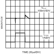
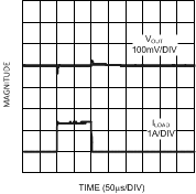
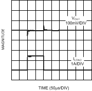
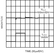
8.2.3 Application Curves