SNVS227H February 2003 – January 2015 LP3872 , LP3875
PRODUCTION DATA.
- 1 Features
- 2 Applications
- 3 Description
- 4 Revision History
- 5 Pin Configuration and Functions
- 6 Specifications
- 7 Detailed Description
-
8 Application and Implementation
- 8.1 Application Information
- 8.2
Typical Application
- 8.2.1 Design Requirements
- 8.2.2 Detailed Design Procedure
- 8.2.3 Application Curves
- 9 Power Supply Recommendations
- 10Layout
- 11Device and Documentation Support
- 12Mechanical, Packaging, and Orderable Information
Package Options
Mechanical Data (Package|Pins)
Thermal pad, mechanical data (Package|Pins)
- KTT|5
Orderable Information
7 Detailed Description
7.1 Overview
The LP387x linear regulators are designed to provide an ultra-low-dropout voltage with excellent transient response and load/line regulation. For battery-powered always-on type applications, the very low quiescent current of LP387x in shutdown mode helps reduce battery drain. For applications where load is not placed close to the regulator, LP3875 incorporates a voltage sense circuit to improve voltage regulation at the point of load. ERROR output pin of LP3872 can be used in the system to flag a low-voltage condition.
7.2 Functional Block Diagram
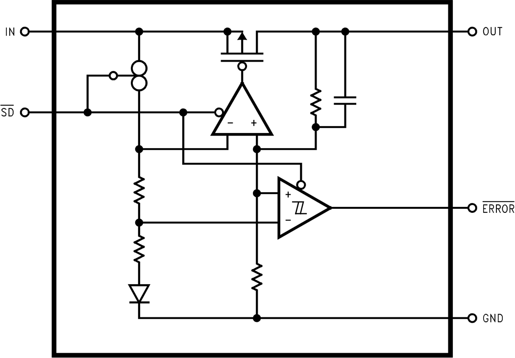 Figure 8. LP3872
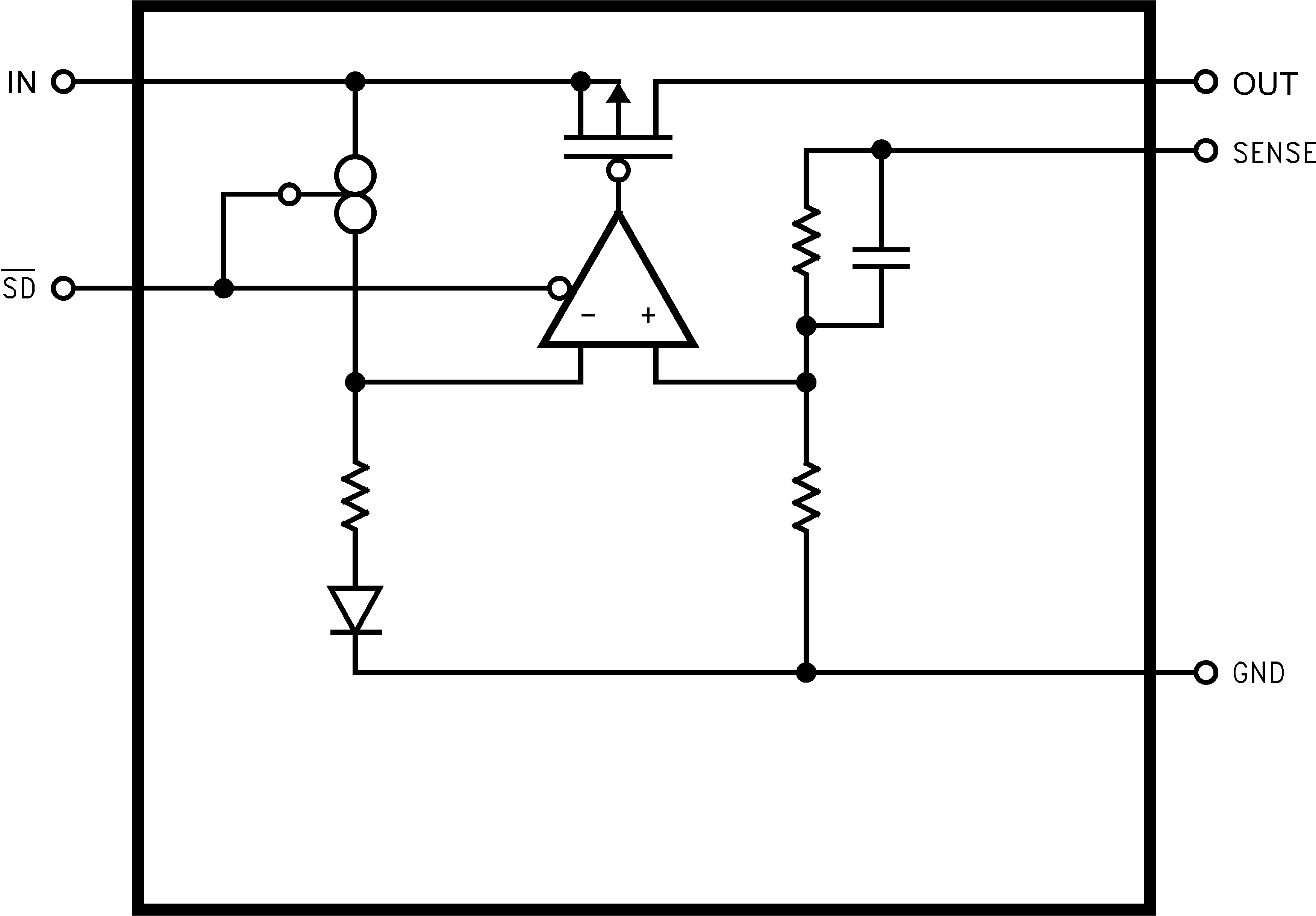 Figure 9. LP3875
7.3 Feature Description
7.3.1 Shutdown (SD)
The LM387x devices have a shutdown feature that turns the device off and reduces the quiescent current to 10 nA, typical.
7.3.2 Load Voltage Sense
In applications where the regulator output is not very close to the load, LP3875 can provide better remote load regulation using the SENSE pin. Figure 10 depicts the advantage of the SENSE option. LP3872 regulates the voltage at the OUT pin. Hence, the voltage at the remote load will be the regulator output voltage minus the drop across the trace resistance. For example, in the case of a 3.3-V output, if the trace resistance is 100 mΩ, the voltage at the remote load will be 3.15 V with 1.5 A of load current, ILOAD. The LP3875 regulates the voltage at the sense pin. Connecting the sense pin to the remote load will provide regulation at the remote load, as shown in Figure 10. If the sense option pin is not required, the SENSE pin must be connected to the OUT pin.
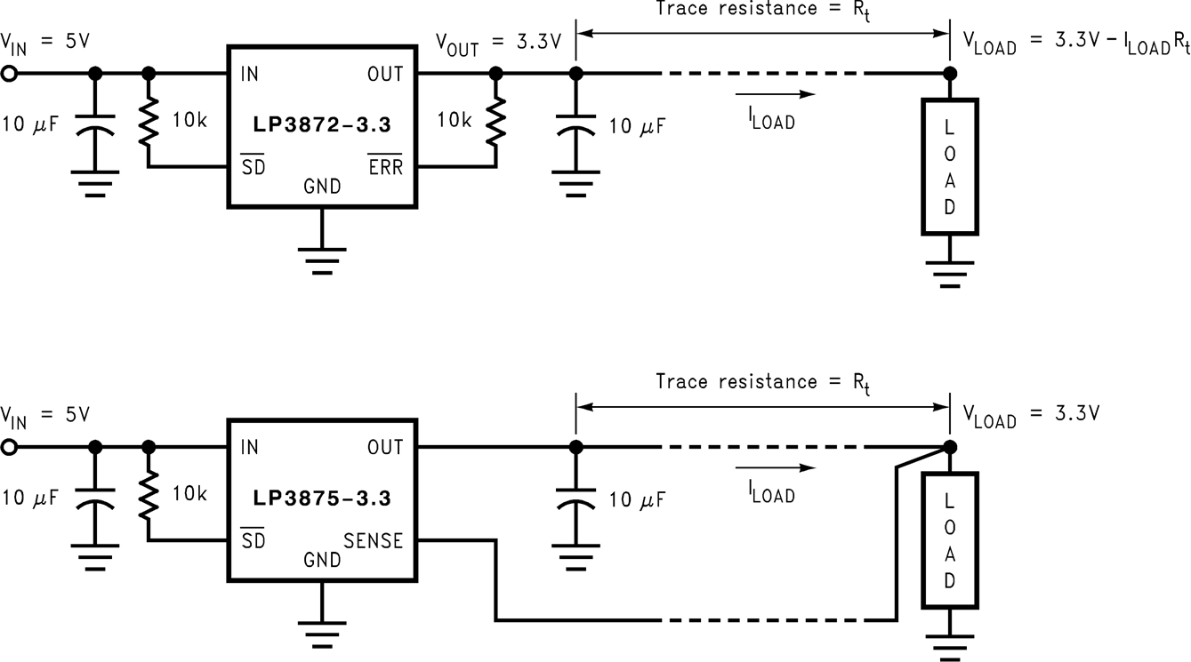 Figure 10. Improving Remote Load Regulation Using LP3875
7.3.3 Short-Circuit Protection
The LP3872 and LP3875 devices are short-circuit protected and in the event of a peak overcurrent condition, the short-circuit control loop will rapidly drive the output PMOS pass element off. Once the power pass element shuts down, the control loop will rapidly cycle the output on and off until the average power dissipation causes the thermal shutdown circuit to respond to servo the on/off cycling to a lower frequency.
7.3.4 Low Dropout Voltage
The LP387x devices feature an ultra-low-dropout voltage, typically 38 mV at 150-mA load current and 380 mV at 1.5-A load current.
7.4 Device Functional Modes
7.4.1 Shutdown Mode
A CMOS Logic low level signal at the shutdown (SD) pin will turn off the regulator. The SD pin must be actively terminated through a 10-kΩ pullup resistor for a proper operation. If this pin is driven from a source that actively pulls high and low (such as a CMOS rail to rail comparator), the pullup resistor is not required. This pin must be tied to VIN if not used.
7.4.2 Active Mode
When voltage at SD pin of the LP387x device is at logic high level, the device is in normal mode of operation.
7.4.3 ERROR Flag Operation
The LP3872 and LP3875 produces a logic low signal at the ERROR Flag pin when the output drops out of regulation due to low input voltage, current limiting, or thermal limiting. This flag has a built-in hysteresis. The timing diagram in Figure 11 shows the relationship between the ERROR flag and the output voltage. In this example, the input voltage is changed to demonstrate the functionality of the ERROR Flag.
The internal ERROR flag comparator has an open-drain output stage. Hence, the ERROR pin should be pulled high through a pullup resistor. Although the ERROR flag pin can sink current of 1 mA, this current is energy drain from the input supply. Hence, the value of the pullup resistor should be in the range of 10 kΩ to 1 MΩ. The ERROR pin must be connected to ground if this function is not used. It should also be noted that when the SD pin is pulled low, the ERROR pin is forced to be invalid for reasons of saving power in shutdown mode.
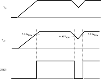 Figure 11. ERROR Flag Operation