SNVS227H February 2003 – January 2015 LP3872 , LP3875
PRODUCTION DATA.
- 1 Features
- 2 Applications
- 3 Description
- 4 Revision History
- 5 Pin Configuration and Functions
- 6 Specifications
- 7 Detailed Description
-
8 Application and Implementation
- 8.1 Application Information
- 8.2
Typical Application
- 8.2.1 Design Requirements
- 8.2.2 Detailed Design Procedure
- 8.2.3 Application Curves
- 9 Power Supply Recommendations
- 10Layout
- 11Device and Documentation Support
- 12Mechanical, Packaging, and Orderable Information
Package Options
Mechanical Data (Package|Pins)
Thermal pad, mechanical data (Package|Pins)
- KTT|5
Orderable Information
6 Specifications
6.1 Absolute Maximum Ratings(1)(2)
If Military/Aerospace specified devices are required, contact the Texas Instruments Sales Office/Distributors for availability and specifications.| MIN | MAX | UNIT | |
|---|---|---|---|
| Lead temperature (soldering, 5 sec.) | 260 | °C | |
| Power dissipation(3) | Internally limited | ||
| IN pin to GND pin voltage | −0.3 | 7.5 | V |
| Shutdown (SD) pin to GND pin voltage | −0.3 | 7.5 | V |
| OUT pin to GND pin voltage(4), (5) | −0.3 | 6 | V |
| IOUT | Short-circuit protected | ||
| ERROR pin to GND pin voltage | VIN | V | |
| SENSE pin to GND pin voltage | VOUT | V | |
| Storage temperature, Tstg | −65 | 150 | °C |
(1) Stresses beyond those listed under Absolute Maximum Ratings may cause permanent damage to the device. These are stress ratings only, which do not imply functional operation of the device at these or any other conditions beyond those indicated under Recommended Operating Conditions. Exposure to absolute-maximum-rated conditions for extended periods may affect device reliability.
(2) If Military/Aerospace specified devices are required, please contact the TI Sales Office/Distributors for availability and specifications.
(3) Internal thermal shutdown circuitry protects the device from permanent damage.
(4) If used in a dual-supply system where the regulator load is returned to a negative supply, the output must be diode-clamped to ground.
(5) The output PMOS structure contains a diode between the IN and OUT pins. This diode is normally reverse biased. This diode will get forward biased if the voltage at the output terminal is forced to be higher than the voltage at the input terminal. This diode can typically withstand 200 mA of DC current and 1 A of peak current.
6.2 ESD Ratings
| VALUE | UNIT | |||
|---|---|---|---|---|
| V(ESD) | Electrostatic discharge | Human body model (HBM), per ANSI/ESDA/JEDEC JS-001(1) | ±2000 | V |
6.3 Recommended Operating Conditions
| MIN | MAX | UNIT | |
|---|---|---|---|
| VIN supply voltage (1) | 2.5 | 7 | V |
| Shutdown (SD) voltage | −0.3 | 7 | V |
| Maximum operating current (DC) IOUT | 1.5 | A | |
| Junction temperature | –40 | 125 | °C |
(1) The minimum operating value for VIN is equal to either [VOUT(NOM) + VDROPOUT] or 2.5 V, whichever is greater.
6.4 Thermal Information
| THERMAL METRIC(1) | LP3872, LP3875 | LP3875 | UNIT | ||
|---|---|---|---|---|---|
| NDC (SOT-223) | KTT (TO-263) | NDH (TO-220) | |||
| 5 PINS | 5 PINS | 5 PINS | |||
| RθJA | Junction-to-ambient thermal resistance | 65.2 | 40.3 | 32 | °C/W |
| RθJC(top) | Junction-to-case (top) thermal resistance | 47.2 | 43.4 | 43.8 | |
| RθJB | Junction-to-board thermal resistance | 9.9 | 23.1 | 18.6 | |
| ψJT | Junction-to-top characterization parameter | 3.4 | 11.5 | 8.8 | |
| ψJB | Junction-to-board characterization parameter | 9.7 | 22 | 18 | |
| RθJC(bot) | Junction-to-case (bottom) thermal resistance | n/a | 1 | 1.2 | |
(1) For more information about traditional and new thermal metrics, see the IC Package Thermal Metrics application report, SPRA953.
6.5 Electrical Characteristics
Unless otherwise specified: TJ = 25°C, VIN = VO(NOM) + 1 V, IL = 10 mA, COUT = 10 µF, VSD = 2 V.| PARAMETER | TEST CONDITIONS | MIN(1) | TYP(2) | MAX(1) | UNIT | |
|---|---|---|---|---|---|---|
| VOUT | Output voltage tolerance (3) | VOUT +1 V ≤ VIN ≤ 7 V, 10 mA ≤ IL ≤ 1.5 A | –1.5% | 0% | 1.5% | |
| VOUT +1 V ≤ VIN ≤ 7 V, 10 mA ≤ IL ≤ 1.5 A, –40°C ≤ TJ ≤ 125°C | –3% | 3% | ||||
| ΔVOL | Output voltage line regulation (3) | VOUT + 1 V ≤ VIN ≤ 7 V | 0.02% | |||
| VOUT + 1 V ≤ VIN ≤ 7 V, –40°C ≤ TJ ≤ 125°C | 0.06% | |||||
| ΔVO/ ΔIOUT | Output voltage load regulation (3) | 10 mA ≤ IL ≤ 1.5 A | 0.06% | |||
| 10 mA ≤ IL ≤ 1.5 A, –40°C ≤ TJ ≤ 125°C | 0.12% | |||||
| VIN - VOUT | Dropout voltage (4) | IL = 150 mA | 38 | 50 | mV | |
| IL = 150 mA, –40°C ≤ TJ ≤ 125°C | 60 | |||||
| IL = 1.5 A | 380 | 450 | ||||
| IL = 1.5 A, –40°C ≤ TJ ≤ 125°C | 550 | |||||
| IGND | Ground pin current in normal operation mode | IL = 150 mA | 5 | 9 | mA | |
| IL = 150 mA,–40°C ≤ TJ ≤ 125°C | 10 | |||||
| IL = 1.5 A | 6 | 14 | ||||
| IL = 1.5 A, –40°C ≤ TJ ≤ 125°C | 15 | |||||
| IGND | Ground pin current in shutdown mode | VSD ≤ 0.3 V | 0.01 | 10 | µA | |
| –40°C ≤ TJ ≤ 85°C | 50 | |||||
| IO(PK) | Peak output current | VOUT ≥ VO(NOM) – 4% | 1.8 | A | ||
| SHORT CIRCUIT PROTECTION | ||||||
| ISC | Short-circuit current | 3.2 | A | |||
| SHUTDOWN INPUT | ||||||
| VSDT | Shutdown threshold | Output = High | VIN | V | ||
| Output = High, –40°C ≤ TJ ≤ 125°C | 2 | |||||
| Output = Low | 0 | |||||
| Output = Low, –40°C ≤ TJ ≤ 125°C | 0.3 | |||||
| TdOFF | Turnoff delay | IL = 1.5 A | 20 | µs | ||
| TdON | Turnon delay | IL = 1.5 A | 25 | µs | ||
| ISD | SD input current | VSD = VIN | 1 | nA | ||
| ERROR FLAG | ||||||
| VT | Threshold | See(5) | 10% | |||
| See(5), –40°C ≤ TJ ≤ 125°C | 5% | 16% | ||||
| VTH | Threshold hysteresis | See(5) | 5% | |||
| See(5), –40°C ≤ TJ ≤ 125°C | 2% | 8% | ||||
| VEF(Sat) | ERROR flag saturation | Isink = 100 µA | 0.02 | V | ||
| Isink = 100 µA, –40°C ≤ TJ ≤ 125°C | 0.1 | |||||
| Td | Flag reset delay | 1 | µs | |||
| Ilk | ERROR flag pin leakage current | 1 | nA | |||
| Imax | ERROR flag pin sink current | VError = 0.5 V | 1 | mA | ||
| AC PARAMETERS | ||||||
| PSRR | Ripple rejection | VIN = VOUT + 1 V, COUT = 10 µF VOUT = 3.3 V, f = 120 Hz |
73 | dB | ||
| VIN = VOUT + 0.5 V, COUT = 10 µF VOUT = 3.3 V, f = 120 Hz |
57 | |||||
| ρn(l/f) | Output noise density | f = 120 Hz | 0.8 | µV | ||
| en | Output noise voltage | BW = 10 Hz – 100 kHz, VOUT = 2.5 V | 150 | µV (rms) | ||
| BW = 300 Hz – 300 kH, VOUT = 2.5 V | 100 | |||||
(1) Limits are specified by testing, design, or statistical correlation.
(2) Typical numbers are at 25°C and represent the most likely parametric norm.
(3) Output voltage line regulation is defined as the change in output voltage from the nominal value due to change in the input line voltage. Output voltage load regulation is defined as the change in output voltage from the nominal value due to change in load current. The line and load regulation specification contains only the typical number. However, the limits for line and load regulation are included in the output voltage tolerance specification.
(4) Dropout voltage is defined as the minimum input to output differential voltage at which the output drops 2% below the nominal value. Dropout voltage specification applies only to output voltages of 2.5 V and above. For output voltages below 2.5 V, the dropout voltage is nothing but the input to output differential, because the minimum input voltage is 2.5 V.
(5) ERROR Flag threshold and hysteresis are specified as percentage of regulated output voltage. See ERROR Flag Operation.
6.6 Typical Characteristics
Unless otherwise specified: TJ = 25°C, COUT = 10 µF, CIN = 10 µF, SD pin is tied to VIN, VOUT = 2.5 V, VIN = VO(NOM) + 1 V, IL = 10 mA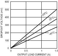 Figure 1. Dropout Voltage vs Output Load Current
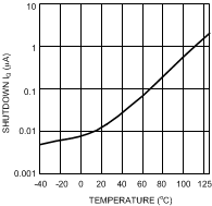 Figure 3. Shutdown IQ vs Junction Temperature
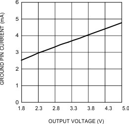 Figure 2. Ground Current vs Output Voltage
IL = 1.5 A
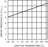 Figure 4. Errorflag Threshold vs Junction Temperature
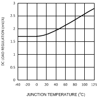 Figure 5. DC Load Reg. vs Junction Temperature
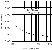 Figure 7. Noise vs Frequency
 Figure 6. DC Line Regulation vs Temperature