SNVSA55C December 2014 – January 2018 LP3907-Q1
PRODUCTION DATA.
- 1 Features
- 2 Applications
- 3 Description
- 4 Revision History
- 5 Device Comparison Tables
- 6 Pin Configuration and Functions
-
7 Specifications
- 7.1 Absolute Maximum Ratings
- 7.2 ESD Ratings
- 7.3 Recommended Operating Conditions (Bucks)
- 7.4 Thermal Information
- 7.5 General Electrical Characteristics
- 7.6 Low Dropout Regulators, LDO1 And LDO2
- 7.7 Buck Converters SW1, SW2
- 7.8 I/O Electrical Characteristics
- 7.9 Power-On Reset (POR) Threshold/Function
- 7.10 I2C Interface Timing Requirements
- 7.11 Typical Characteristics — LDO
- 7.12 Typical Characteristics — Bucks
- 7.13 Typical Characteristics — Buck1
- 7.14 Typical Characteristics — Buck2
- 7.15 Typical Characteristics — Bucks
-
8 Detailed Description
- 8.1 Overview
- 8.2 Functional Block Diagram
- 8.3
Feature Description
- 8.3.1 DC-DC Converters
- 8.3.2
SW1, SW2: Synchronous Step-Down Magnetic DC-DC Converters
- 8.3.2.1 Functional Description
- 8.3.2.2 Circuit Operation Description
- 8.3.2.3 PWM Operation
- 8.3.2.4 Internal Synchronous Rectification
- 8.3.2.5 Current Limiting
- 8.3.2.6 PFM Operation
- 8.3.2.7 SW1, SW2 Operation
- 8.3.2.8 SW1, SW2 Control Registers
- 8.3.2.9 Soft Start
- 8.3.2.10 Low Dropout Operation
- 8.3.2.11 Flexible Power Sequencing of Multiple Power Supplies
- 8.3.2.12 Power-Up Sequencing Using the EN_T Function
- 8.3.3 Flexible Power-On Reset (Power Good with Delay)
- 8.3.4 Undervoltage Lockout
- 8.4 Device Functional Modes
- 8.5 Programming
- 8.6
Register Maps
- 8.6.1
LP3907-Q1 Control Registers
- 8.6.1.1 Interrupt Status Register (ISRA) 0x02
- 8.6.1.2 Control 1 Register (SCR1) 0x07
- 8.6.1.3 EN_DLY Preset Delay Sequence After EN_T Assertion
- 8.6.1.4 Buck and LDO Output Voltage Enable Register (BKLDOEN) – 0x10
- 8.6.1.5 Buck and LDO Status Register (BKLDOSR) – 0x11
- 8.6.1.6 Buck Voltage Change Control Register 1 (VCCR) – 0x20
- 8.6.1.7 Buck1 Target Voltage 1 Register (B1TV1) – 0x23
- 8.6.1.8 Buck1 Target Voltage 2 Register (B1TV2) – 0x24
- 8.6.1.9 Buck1 Ramp Control Register (B1RC) - 0x25
- 8.6.1.10 Buck2 Target Voltage 1 Register (B2TV1) – 0x29
- 8.6.1.11 Buck2 Target Voltage 2 Register (B2TV2) – 0x2A
- 8.6.1.12 Buck2 Ramp Control Register (B2RC) - 0x2B
- 8.6.1.13 Buck Function Register (BFCR) – 0x38
- 8.6.1.14 LDO1 Control Register (LDO1VCR) – 0x39
- 8.6.1.15 LDO2 Control Register (LDO2VCR) – 0x3A
- 8.6.1
LP3907-Q1 Control Registers
- 9 Application and Implementation
- 10Power Supply Recommendations
- 11Layout
- 12Device and Documentation Support
- 13Mechanical, Packaging, and Orderable Information
Package Options
Mechanical Data (Package|Pins)
Thermal pad, mechanical data (Package|Pins)
- RTW|24
Orderable Information
9.2.2.2.3 Capacitor Characteristics
The LDOs are designed to work with ceramic capacitors on the output to take advantage of the benefits they offer. For capacitance values in the range of 0.47 µF to 4.7 µF, ceramic capacitors are the smallest, least expensive and have the lowest ESR values, thus making them best for eliminating high frequency noise. The ESR of a typical 1-µF ceramic capacitor is in the range of 20 mΩ to 40 mΩ, which easily meets the ESR requirement for stability for the LDOs.
For both input and output capacitors, careful interpretation of the capacitor specification is required to ensure correct device operation. The capacitor value can change greatly, depending on the operating conditions and capacitor type.
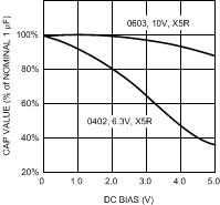
In particular, the output capacitor selection should take account of all the capacitor parameters, to ensure that the specification is met within the application. The capacitance can vary with DC bias conditions as well as temperature and frequency of operation. Capacitor values will also show some decrease over time due to aging. The capacitor parameters are also dependent on the particular case size, with smaller sizes giving poorer performance figures in general. As an example, Figure 46 is a typical graph comparing different capacitor case sizes.
 Figure 46. Graph Showing Typical Variation in Capacitance vs. DC Bias
As shown in the graph, increasing the DC Bias condition can result in the capacitance value that falls below the minimum value given in the recommended capacitor specifications table. Note that the graph shows the capacitance out of spec for the 0402 case size capacitor at higher bias voltages. It is therefore recommended that the capacitor manufacturers' specifications for the nominal value capacitor are consulted for all conditions, as some capacitor sizes (for example, 0402) may not be suitable in the actual application.
The ceramic capacitor’s capacitance can vary with temperature. The capacitor type X7R, which operates over a temperature range of −55°C to 125°C, only varies the capacitance to within ±15%. The capacitor type X5R has a similar tolerance over a reduced temperature range of −55°C to 85°C. Many large value ceramic capacitors, larger than 1 µF are manufactured with Z5U or Y5V temperature characteristics. Their capacitance can drop by more than 50% as the temperature varies from 25°C to 85°C. Therefore, X7R is recommended over Z5U and Y5V in applications where the ambient temperature changes significantly above or below 25°C.
Tantalum capacitors are less desirable than ceramic for use as output capacitors because they are more expensive when comparing equivalent capacitance and voltage ratings in the 0.47-µF to 4.7-µF range.
Another important consideration is that tantalum capacitors have higher ESR values than equivalent size ceramics. This means that while it may be possible to find a tantalum capacitor with an ESR value within the stable range, it would have to be larger in capacitance (which means bigger and more costly) than a ceramic capacitor with the same ESR value. Note, also, that the ESR of a typical tantalum increases about 2:1 as the temperature goes from 25°C down to −40°C, so some guard band must be allowed.