SNVS550E September   2009  – January 2017 LP5523

PRODUCTION DATA.  

  1. Features
  2. Applications
  3. Description
  4. Revision History
  5. Pin Configuration and Functions
  6. Specifications
    1. 6.1  Absolute Maximum Ratings
    2. 6.2  ESD Ratings
    3. 6.3  Recommended Operating Conditions
    4. 6.4  Thermal Information
    5. 6.5  Electrical Characteristics
    6. 6.6  Charge Pump Electrical Characteristics
    7. 6.7  LED Driver Electrical Characteristics
    8. 6.8  LED Test Electrical Characteristics
    9. 6.9  Logic Interface Characteristics
    10. 6.10 Recommended External Clock Source Conditions
    11. 6.11 Serial Bus Timing Parameters (SDA, SCL)
    12. 6.12 Typical Characteristics
  7. Detailed Description
    1. 7.1 Overview
    2. 7.2 Functional Block Diagram
    3. 7.3 Feature Description
      1. 7.3.1 Programming
      2. 7.3.2 LED Error Detection
      3. 7.3.3 Energy Efficiency
      4. 7.3.4 Temperature Compensation
      5. 7.3.5 Charge Pump Operational Description
        1. 7.3.5.1 Overview
        2. 7.3.5.2 Output Resistance
        3. 7.3.5.3 Controlling The Charge Pump
        4. 7.3.5.4 LED Forward Voltage Monitoring
        5. 7.3.5.5 Gain Change Hysteresis
      6. 7.3.6 LED Driver Operational Description
        1. 7.3.6.1 Overview
        2. 7.3.6.2 Powering LEDs
        3. 7.3.6.3 Controlling The High-Side LED Drivers
    4. 7.4 Device Functional Modes
      1. 7.4.1 Modes Of Operation
        1. 7.4.1.1 Automatic Power-Save Mode
        2. 7.4.1.2 PWM Power-Save Mode
    5. 7.5 Programming
      1. 7.5.1 I2C-Compatible Control Interface
        1. 7.5.1.1 Data Validity
        2. 7.5.1.2 Start and Stop Conditions
        3. 7.5.1.3 Transferring Data
        4. 7.5.1.4 I2C-Compatible Chip Address
          1. 7.5.1.4.1 Control Register Write Cycle
          2. 7.5.1.4.2 Control Register Read Cycle
          3. 7.5.1.4.3 Auto-Increment Feature
    6. 7.6 Register Maps
      1. 7.6.1 Register Set
      2. 7.6.2 Control Register Details
      3. 7.6.3 Instruction Set
      4. 7.6.4 LED Driver Instructions
        1. 7.6.4.1 Ramp
        2. 7.6.4.2 Ramp Instruction Application Example
        3. 7.6.4.3 Set_PWM
        4. 7.6.4.4 Wait
      5. 7.6.5 LED Mapping Instructions
      6. 7.6.6 Branch Instructions
      7. 7.6.7 Arithmetic Instructions
  8. Application and Implementation
    1. 8.1 Application Information
    2. 8.2 Typical Applications
      1. 8.2.1 Using Two LP5523 Devices in Same Application
        1. 8.2.1.1 Design Requirements
        2. 8.2.1.2 Detailed Design Procedure
          1. 8.2.1.2.1 Recommended External Components
        3. 8.2.1.3 Application Curves
      2. 8.2.2 Driving Haptic Feedback with LP5523
  9. Power Supply Recommendations
  10. 10Layout
    1. 10.1 Layout Guidelines
    2. 10.2 Layout Example
  11. 11Device and Documentation Support
    1. 11.1 Device Support
      1. 11.1.1 Third-Party Products Disclaimer
    2. 11.2 Receiving Notification of Documentation Updates
    3. 11.3 Community Resources
    4. 11.4 Trademarks
    5. 11.5 Electrostatic Discharge Caution
    6. 11.6 Glossary
  12. 12Mechanical, Packaging, and Orderable Information

Package Options

Mechanical Data (Package|Pins)
Thermal pad, mechanical data (Package|Pins)
Orderable Information

Layout

Layout Guidelines

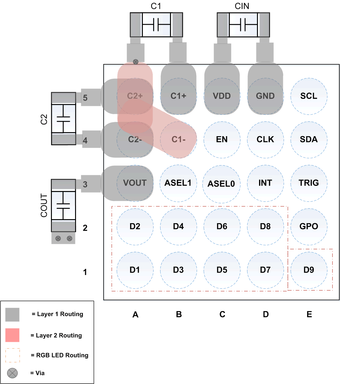
Place capacitors as close as possible to the LP5523 device to minimize the current loops. Example of LP5523 PCB layout and component placement is seen in Figure 31.

Layout Example

LP5523 layout_snvs550.gif Figure 31. LP5523 Layout Example