SNVS873E August 2012 – November 2016 LP5560
PRODUCTION DATA.
- 1 Features
- 2 Applications
- 3 Description
- 4 Revision History
- 5 Pin Configuration and Functions
- 6 Specifications
-
7 Detailed Description
- 7.1 Overview
- 7.2 Functional Block Diagram
- 7.3 Feature Description
- 7.4 Device Functional Modes
- 7.5 Programming
- 7.6 Registers
- 8 Application and Implementation
- 9 Power Supply Recommendations
- 10Layout
- 11Device and Documentation Support
- 12Mechanical, Packaging, and Orderable Information
Package Options
Mechanical Data (Package|Pins)
- YFQ|4
Thermal pad, mechanical data (Package|Pins)
Orderable Information
1 Features
- Wide Input-Voltage Range: 2.7 V to 5.5 V
- Adjustable Output Current: 2.8 mA to 19.5 mA
- Programmable Blinking Sequence with Current Rise and Fall Time Control
- Default Blinking Sequence for Simple Systems Without Programming Capabilities
- Single-Wire Interface
- Constant Current High Side Output Driver
- Very Low Headroom Voltage (40 mV Typical)
- Ultra-Small Solution Size – No External Components
2 Applications
- Indicator LEDs in Cell Phones and Other Portable Devices
- Card Readers
- Fuel Dispensers
- Pedometers
- Electronic Access Control
- Where Simple Feedback is Needed
3 Description
The LP5560 is a programmable LED driver that can generate variety of blinking sequences with up to three pulses of different length per sequence. Blinking sequences can be programmed through a single-wire interface. Programmable parameters include on and off times as well as rise and fall times. Default sequence is programmed into the LP5560 to enable the use of device in simple systems without programming capabilities.
Very low headroom voltage eliminates the need for a boost converter. Indicator LEDs can be driven directly from the battery. Small package size combined with zero external components minimizes the solution size.
LP5560 is available in TI’s tiny 4-pin DSBGA package with 0.4-mm pitch.
Device Information(1)
| PART NUMBER | PACKAGE | BODY SIZE (NOM) |
|---|---|---|
| LP5560 | DSBGA (4) | 0.886 mm × 0.886 mm |
- For all available packages, see the orderable addendum at the end of the data sheet.
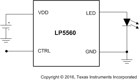
Typical Application
