SNVS873E August 2012 – November 2016 LP5560
PRODUCTION DATA.
- 1 Features
- 2 Applications
- 3 Description
- 4 Revision History
- 5 Pin Configuration and Functions
- 6 Specifications
-
7 Detailed Description
- 7.1 Overview
- 7.2 Functional Block Diagram
- 7.3 Feature Description
- 7.4 Device Functional Modes
- 7.5 Programming
- 7.6 Registers
- 8 Application and Implementation
- 9 Power Supply Recommendations
- 10Layout
- 11Device and Documentation Support
- 12Mechanical, Packaging, and Orderable Information
Package Options
Mechanical Data (Package|Pins)
- YFQ|4
Thermal pad, mechanical data (Package|Pins)
Orderable Information
8 Application and Implementation
NOTE
Information in the following applications sections is not part of the TI component specification, and TI does not warrant its accuracy or completeness. TI’s customers are responsible for determining suitability of components for their purposes. Customers should validate and test their design implementation to confirm system functionality.
8.1 Application Information
The LP5560 is a programmable LED driver designed to generate variety of blinking sequences for indicator LEDs. It can drive single LED with up to 19.5 mA output current. Very low headroom voltage allows driving most indicator LEDs straight from a single Li-ion battery. Default blinking sequence with one pulse is programmed into the LP5560 to enable the use of device in simple systems without programming capabilities. Pulling CTRL signal high starts the default blinking sequence. Different blinking sequences with up to three pulses can be programmed into the LP5560 through a single-wire interface. Programmable parameters include on and off times as well as rise and fall times.
8.2 Typical Application
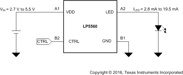 Figure 18. LP5560 Typical Application
8.2.1 Design Requirements
In this example LP5560 is used to drive a blue 0406-size indicator LED with a 5.3-mA output current. For this example, use the parameters listed in Table 7.
Table 7. Design Parameters
| DESIGN PARAMETER | EXAMPLE VALUE |
|---|---|
| LED Output Current | 5.3 mA |
| Maximum LED forward voltage at 5 mA | 3.1 V |
| VIN voltage | from 3.2 V to 5.5 V |
8.2.2 Detailed Design Procedure
8.2.2.1 Step-by-Step Design Procedure
To design in the LP5560 use the following simple design steps:
- Define the input voltage range of the system. For the LP5560 device the maximum input voltage must not exceed 5.5 V. The minimum input voltage is critical parameter for LED selection.
- Define the LED current. LED current affects the LED forward voltage and must be taken into account when selecting the LED for the application.
- Choose a LED which maximum forward voltage with desired LED current is less than minimum input voltage - 100 mV. This ensures that there is always enough headroom voltage available for the LED driver.
8.2.2.2 Running the Default Blinking Sequence
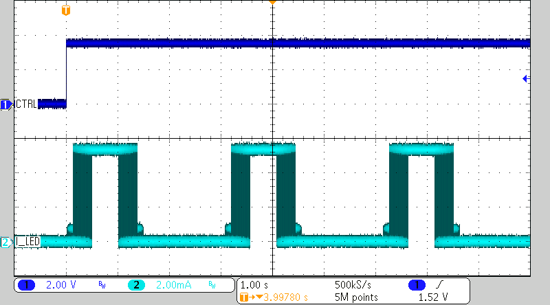
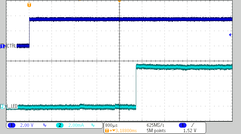
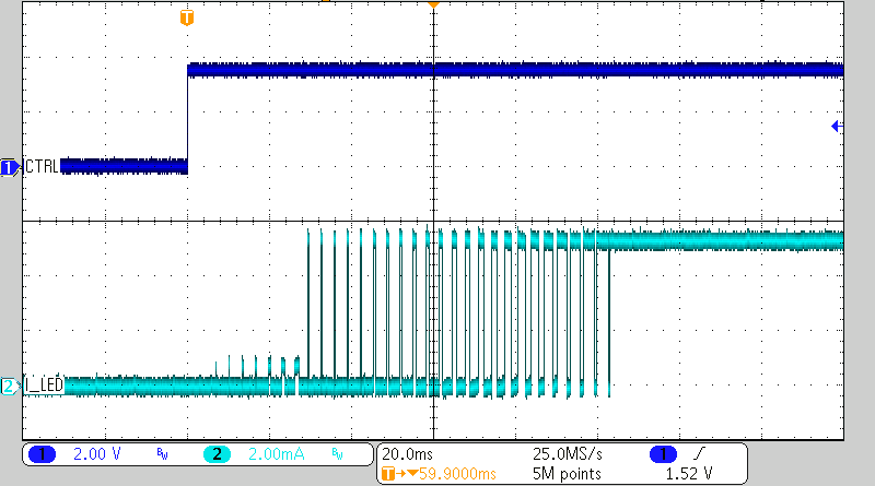
To run the default blinking sequence apply input voltage to VDD pin. Allow the VDD voltage settle before pulling the CTRL pin high. It is not recommended to connect the CTRL and VDD lines together. When CTRL line is pulled high the LP5560 starts to generate the default blinking sequence. Figure 19 shows the LP5560 generating default sequence. Rise and fall times are generated using a combined PWM and current control. Ramp has 32 PWM steps. For the first 8 steps LED current is decreased to 12.5%. For the remaining steps current is set to 100%. Each step is 3.3 ms long. This result’s the minimum ramp time of 3.3 ms × 32 = 105.6 ms. Figure 22 shows LED current with minimum rise time. When ramp time is increased each PWM step is done multiple times. In the default sequence rise and fall times are set to 528 ms.
8.2.2.3 Programming New Blinking Sequence to the Memory
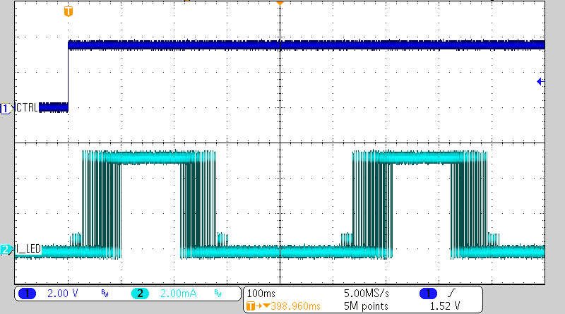
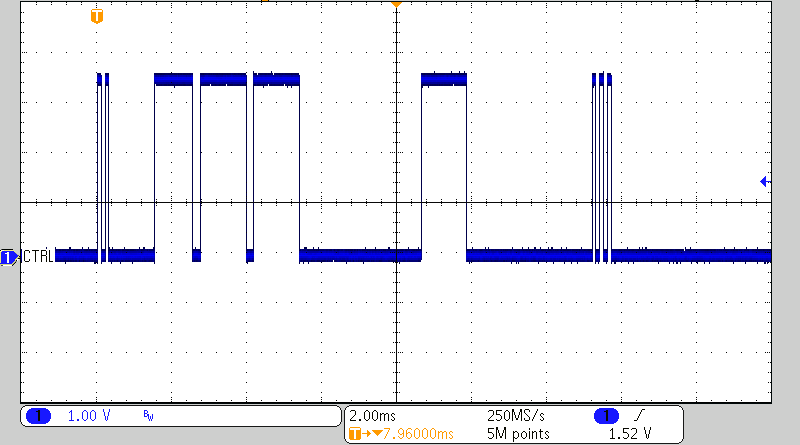
Figure 22 shows an example of a training sequence which programs a new blinking sequence into the LP5560 memory. This example has a single pulse with 105.6 ms rise time, 105.6 ms on time, 105.6 ms fall time and 211.2 ms off time. LED current is set to 5.3 mA. Training sequence is started by giving a training start command (two rising edges within 500 µs). First pulse after a training start command is the calibration pulse which determines the speed of the training sequence. Note that there must always be at least 1500 µs from the first rising edge of the training start command before calibration pulse can be given. Second pulse after the calibration pulse is the LED current setting. Note that there are empty low times before and after current setting pulse. For the following pulses both CTRL high and CTRL low times are used to set the parameters. Next CTRL high time defines LED current rise time setting for pulse 1 (R1). CTRL low time after R1 defines the LED on time for pulse 1 (ON1). CTRL high time after ON1 sets the LED current fall time (F1). CTRL low time after F1 sets pulse 1 off time (OFF1). The training sequence is finished with a training stop command (three rising edges within 500 µs). Figure 23 show the LED current after programming the new pulse into the LP5560 memory.
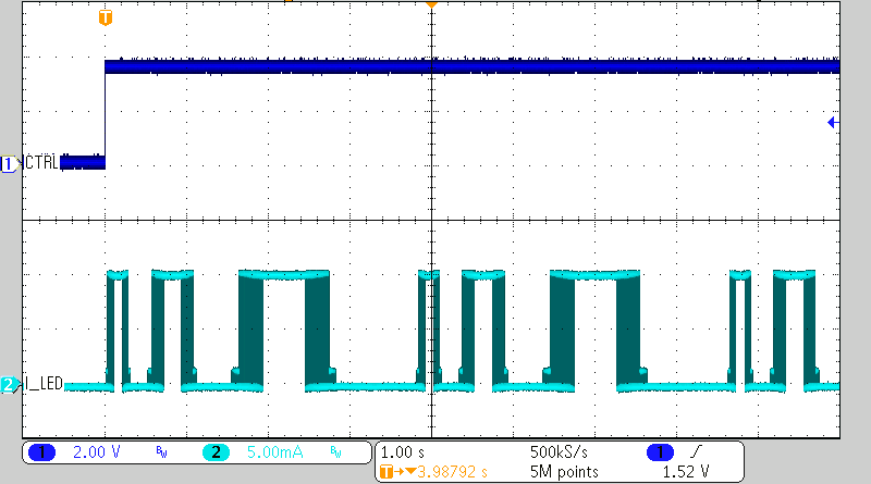
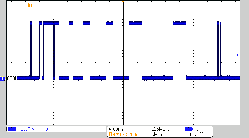
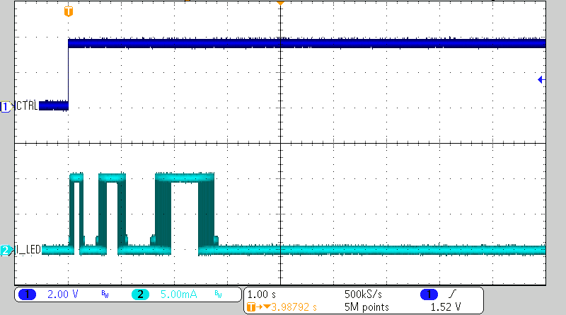
Figure 24 and Figure 25 show another example of a training sequence with three pulses and the resulting blinking sequence. In this example all three pulses have different rise, on, fall, and off times. LED current is set to 10.2 mA. Figure 26 show how this sequence is run only once using the run-once command. Even though the CTRL is held high for a long time the blinking sequence is only executed one time because a run-once command (four rising edges within 500 µs) is given at the beginning of the frame.
8.2.3 Application Curves
