SNVSA91F September 2015 – April 2021 LP5910
PRODUCTION DATA
- 1 Features
- 2 Applications
- 3 Description
- 4 Revision History
- 5 Pin Configuration and Functions
- 6 Specifications
- 7 Detailed Description
- 8 Applications and Implementation
- 9 Power Supply Recommendations
- 10Layout
- 11Device and Documentation Support
Package Options
Mechanical Data (Package|Pins)
Thermal pad, mechanical data (Package|Pins)
- DRV|6
Orderable Information
5 Pin Configuration and Functions
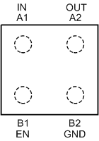
 Figure 5-1 YKA Package,4-Pin Ultra-Thin DSBGA,
Top View
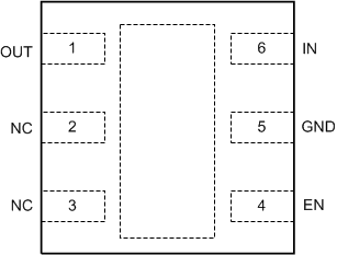
 Figure 5-3 DRV Package,6-Pin WSON With Thermal Pad,Top
View
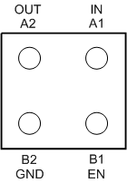
 Figure 5-2 YKA Package,4-Pin Ultra-Thin DSBGA,
Bottom View
Figure 5-2 YKA Package,4-Pin Ultra-Thin DSBGA,
Bottom ViewTable 5-1 Pin Functions
| PIN | I/O | DESCRIPTION | ||
|---|---|---|---|---|
| NAME | DSBGA | WSON | ||
| EN | B1 | 4 | I | Enable input; disables the regulator when logic low. Enables the regulator when logic high. An internal 1-MΩ pull down resistor connects this input to ground. |
| GND | B2 | 5 | — | Common ground |
| IN | A1 | 6 | I | Voltage supply input. A 1-μF capacitor must be connected at this input. |
| NC | — | 2, 3 | — | No internal connection. Connect to ground or leave open. |
| OUT | A2 | 1 | O | Voltage output. A 1-µF low-ESR capacitor must be connected from this pin to the GND pin. Connect this output to the load circuit. |
| Exposed Pad | — | Thermal Pad | — | The exposed thermal pad on the bottom of the package must be connected to a copper area under the package on the PCB. Connect to ground potential or leave floating. Do not connect to any potential other than the same ground potential seen at device pin 5 (GND). See the Section 8.2.2.8 section for more information. |