SNVSAA8C December 2015 – September 2016 LP5912-Q1
PRODUCTION DATA.
- 1 Features
- 2 Applications
- 3 Description
- 4 Revision History
- 5 Voltage Options
- 6 Pin Configuration and Functions
- 7 Specifications
- 8 Typical Characteristics
- 9 Detailed Description
- 10Applications and Implementation
- 11Power Supply Recommendations
- 12Layout
- 13Device and Documentation Support
- 14Mechanical, Packaging, and Orderable Information
Package Options
Mechanical Data (Package|Pins)
- DRV|6
Thermal pad, mechanical data (Package|Pins)
- DRV|6
Orderable Information
1 Features
- Qualified for Automotive Applications
- AEC Q100-Qualified With the Following Results
- Device Temperature Grade 1: –40°C to +125°C Ambient Operating Temperature Range
- Device HBM Classification Level 2
- Device CDM Classification Level C6
- Input Voltage Range: 1.6 V to 6.5 V
- Output Voltage Range: 0.8 V to 5.5 V
- Output Current up to 500 mA
- Low Output-Voltage Noise: 12 µVRMS Typical
- PSRR at 1 kHz: 75 dB Typical
- Output Voltage Tolerance (VOUT ≥ 3.3 V): ±2%
- Low IQ (Enabled, No Load): 30 µA Typical
- Low Dropout (VOUT ≥ 3.3 V): 95 mV Typical at 500-mA Load
- Stable With 1-µF Ceramic Input and Output Capacitors
- Thermal-Overload and Short-Circuit Protection
- Reverse Current Protection
- No Noise Bypass Capacitor Required
- Output Automatic Discharge for Fast Turnoff
- Power-Good Output With 140-µs Typical Delay
- Internal Soft-Start to Limit the In-rush Current
- –40°C to +125°C Operating Junction Temperature Range
2 Applications
- Automotive Infotainment
- Telematics Systems
- ADAS Cameras and Radar
- Navigation Systems
3 Description
The LP5912-Q1 is low-noise LDO that can supply up to 500 mA of output current. Designed to meet the requirements of RF and analog circuits, the LP5912-Q1 device provides low noise, high PSRR, low quiescent current, and low line and load transient response. The LP5912-Q1 offers class-leading noise performance without a noise bypass capacitor and with the ability for remote output capacitance placement.
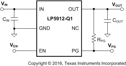
The device is designed to work with a 1-µF input and a 1-µF output ceramic capacitor (no separate noise bypass capacitor required).
This device is available with fixed output voltages from 0.8 V to 5.5 V in 25-mV steps. Contact Texas Instruments Sales for specific voltage option needs.
Device Information(1)
| PART NUMBER | PACKAGE | BODY SIZE (NOM) |
|---|---|---|
| LP5912-Q1 | WSON (6) | 2.00 mm × 2.00 mm |
- For all available packages, see the Package Option Addendum (POA) at the end of this data sheet.
space
space
space
space
space
Simplified Schematic
