SNVSB22 March 2018 LP87561-Q1 , LP87562-Q1 , LP87563-Q1 , LP87564-Q1 , LP87565-Q1
PRODUCTION DATA.
- 1 Features
- 2 Applications
- 3 Description
- 4 Revision History
- 5 Device Comparison Table
- 6 Pin Configuration and Functions
- 7 Specifications
-
8 Detailed Description
- 8.1 Overview
- 8.2 Functional Block Diagram
- 8.3
Feature Descriptions
- 8.3.1 Multi-Phase DC/DC Converters
- 8.3.2 Sync Clock Functionality
- 8.3.3 Power-Up
- 8.3.4 Regulator Control
- 8.3.5 Enable and Disable Sequences
- 8.3.6 Device Reset Scenarios
- 8.3.7 Diagnosis and Protection Features
- 8.3.8 GPIO Signal Operation
- 8.3.9 Digital Signal Filtering
- 8.4 Device Functional Modes
- 8.5 Programming
- 8.6
Register Maps
- 8.6.1
Register Descriptions
- 8.6.1.1 OTP_REV
- 8.6.1.2 BUCK0_CTRL1
- 8.6.1.3 BUCK0_CTRL2
- 8.6.1.4 BUCK1_CTRL1
- 8.6.1.5 BUCK1_CTRL2
- 8.6.1.6 BUCK2_CTRL1
- 8.6.1.7 BUCK2_CTRL2
- 8.6.1.8 BUCK3_CTRL1
- 8.6.1.9 BUCK3_CTRL2
- 8.6.1.10 BUCK0_VOUT
- 8.6.1.11 BUCK0_FLOOR_VOUT
- 8.6.1.12 BUCK1_VOUT
- 8.6.1.13 BUCK1_FLOOR_VOUT
- 8.6.1.14 BUCK2_VOUT
- 8.6.1.15 BUCK2_FLOOR_VOUT
- 8.6.1.16 BUCK3_VOUT
- 8.6.1.17 BUCK3_FLOOR_VOUT
- 8.6.1.18 BUCK0_DELAY
- 8.6.1.19 BUCK1_DELAY
- 8.6.1.20 BUCK2_DELAY
- 8.6.1.21 BUCK3_DELAY
- 8.6.1.22 GPIO2_DELAY
- 8.6.1.23 GPIO3_DELAY
- 8.6.1.24 RESET
- 8.6.1.25 CONFIG
- 8.6.1.26 INT_TOP1
- 8.6.1.27 INT_TOP2
- 8.6.1.28 INT_BUCK_0_1
- 8.6.1.29 INT_BUCK_2_3
- 8.6.1.30 TOP_STAT
- 8.6.1.31 BUCK_0_1_STAT
- 8.6.1.32 BUCK_2_3_STAT
- 8.6.1.33 TOP_MASK1
- 8.6.1.34 TOP_MASK2
- 8.6.1.35 BUCK_0_1_MASK
- 8.6.1.36 BUCK_2_3_MASK
- 8.6.1.37 SEL_I_LOAD
- 8.6.1.38 I_LOAD_2
- 8.6.1.39 I_LOAD_1
- 8.6.1.40 PGOOD_CTRL1
- 8.6.1.41 PGOOD_CTRL2
- 8.6.1.42 PGOOD_FLT
- 8.6.1.43 PLL_CTRL
- 8.6.1.44 PIN_FUNCTION
- 8.6.1.45 GPIO_CONFIG
- 8.6.1.46 GPIO_IN
- 8.6.1.47 GPIO_OUT
- 8.6.1
Register Descriptions
- 9 Application and Implementation
- 10Power Supply Recommendations
- 11Layout
- 12Device and Documentation Support
- 13Mechanical, Packaging, and Orderable Information
Package Options
Refer to the PDF data sheet for device specific package drawings
Mechanical Data (Package|Pins)
- RNF|26
Thermal pad, mechanical data (Package|Pins)
Orderable Information
8.3.4.2 Changing Output Voltage
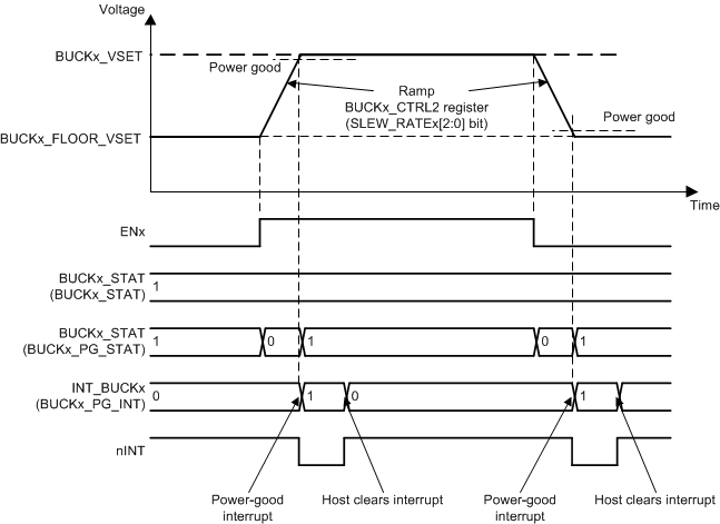
The output voltage of the regulator can be changed by the ENx pin (voltage levels defined by the BUCKx_VOUT and BUCKx_FLOOR_VOUT registers) or by writing to the BUCKx_VOUT and BUCKx_FLOOR_VOUT registers. The voltage change is always slew-rate controlled, and the slew-rate is defined by the SLEW_RATE[2:0] bits (in BUCKx_CTRL2 register). During voltage change the forced-PWM mode is used automatically. If the multiphase operation is forced by the BUCKx_FPWM_MP bit (in BUCKx_CTRL1 register), the regulator operates in multiphase mode (two phases in dual-phase configuration, 3 phases in 3-phase configuration, and 4 phases in 4-phase configuration). If the multiphase operation is not forced, the number of phases are added and shedded automatically to follow the required slew rate. When the programmed output voltage is achieved, the mode becomes the one defined by the load current and the BUCKx_FPWM and BUCKx_FPWM_MP bits in BUCKx_CTRL1 register.
The Power-Good interrupt is generated when the output voltage reaches the programmed voltage level, as shown in Figure 15.
 Figure 15. Regulator Output Voltage Change With ENx pin