SNVSA21G May 2014 – October 2017 LP8860-Q1
PRODUCTION DATA.
- 1 Features
- 2 Applications
- 3 Description
- 4 Revision History
- 5 Device Comparison Table
- 6 Pin Configuration and Functions
-
7 Specifications
- 7.1 Absolute Maximum Ratings
- 7.2 ESD Ratings
- 7.3 Recommended Operating Conditions
- 7.4 Thermal Information
- 7.5 Electrical Characteristics
- 7.6 Current Sinks Electrical Characteristics
- 7.7 Boost Converter Characteristics
- 7.8 Logic Interface Characteristics
- 7.9 VIN Undervoltage Protection (VIN_UVLO)
- 7.10 VDD Undervoltage Protection (VDD_UVLO)
- 7.11 VIN Overvoltage Protection (VIN_OVP)
- 7.12 VIN Overcurrent Protection (VIN_OCP)
- 7.13 Power-Line FET Control Electrical Characteristics
- 7.14 External Temp Sensor Control Electrical Characteristics
- 7.15 I2C Serial Bus Timing Parameters (SDA, SCLK)
- 7.16 SPI Timing Requirements
- 7.17 Typical Characteristics
-
8 Detailed Description
- 8.1 Overview
- 8.2 Functional Block Diagram
- 8.3 Feature Description
- 8.4 Device Functional Modes
- 8.5 Programming
- 8.6
Register Maps
- 8.6.1
Register Bit Explanations
- 8.6.1.1 Display/Cluster1 Brightness Control MSB
- 8.6.1.2 Display/Cluster1 Brightness Control LSB
- 8.6.1.3 Display/Cluster1 Output Current MSB
- 8.6.1.4 Display/Cluster1 Output Current LSB
- 8.6.1.5 Cluster2 Brightness Control MSB
- 8.6.1.6 Cluster2 Brightness Control LSB
- 8.6.1.7 Cluster2 Output Current
- 8.6.1.8 Cluster3 Brightness Control MSB
- 8.6.1.9 Cluster3 Brightness Control LSB
- 8.6.1.10 Cluster3 Output Current
- 8.6.1.11 Cluster4 Brightness Control MSB
- 8.6.1.12 Cluster4 Brightness Control LSB
- 8.6.1.13 Cluster4 Output Current
- 8.6.1.14 Configuration
- 8.6.1.15 Status
- 8.6.1.16 Fault
- 8.6.1.17 LED Fault
- 8.6.1.18 Fault Clear
- 8.6.1.19 Identification
- 8.6.1.20 Temp MSB
- 8.6.1.21 Temp LSB
- 8.6.1.22 Display LED Current MSB
- 8.6.1.23 Display LED Current LSB
- 8.6.1.24 Display LED PWM MSB
- 8.6.1.25 Display LED PWM LSB
- 8.6.1.26 EEPROM Control
- 8.6.1.27 EEPROM Unlock Code
- 8.6.2
EEPROM Bit Explanations
- 8.6.2.1 EEPROM Register 0
- 8.6.2.2 EEPROM Register 1
- 8.6.2.3 EEPROM Register 2
- 8.6.2.4 EEPROM Register 3
- 8.6.2.5 EEPROM Register 4
- 8.6.2.6 EEPROM Register 5
- 8.6.2.7 EEPROM Register 6
- 8.6.2.8 EEPROM Register 7
- 8.6.2.9 EEPROM Register 8
- 8.6.2.10 EEPROM Register 9
- 8.6.2.11 EEPROM Register 10
- 8.6.2.12 EEPROM Register 11
- 8.6.2.13 EEPROM Register 12
- 8.6.2.14 EEPROM Register 13
- 8.6.2.15 EEPROM Register 14
- 8.6.2.16 EEPROM Register 15
- 8.6.2.17 EEPROM Register 16
- 8.6.2.18 EEPROM Register 17
- 8.6.2.19 EEPROM Register 18
- 8.6.2.20 EEPROM Register 19
- 8.6.2.21 EEPROM Register 20
- 8.6.2.22 EEPROM Register 21
- 8.6.2.23 EEPROM Register 22
- 8.6.2.24 EEPROM Register 23
- 8.6.2.25 EEPROM Register 24
- 8.6.1
Register Bit Explanations
-
9 Application and Implementation
- 9.1 Application Information
- 9.2
Typical Applications
- 9.2.1
Typical Application for Display Backlight
- 9.2.1.1 Design Requirements
- 9.2.1.2
Detailed Design Procedure
- 9.2.1.2.1 Inductor Selection
- 9.2.1.2.2 Output Capacitor Selection
- 9.2.1.2.3 Input Capacitor Selection
- 9.2.1.2.4 Charge Pump Output Capacitor
- 9.2.1.2.5 Charge Pump Flying Capacitor
- 9.2.1.2.6 Diode
- 9.2.1.2.7 Boost Converter Transistor
- 9.2.1.2.8 Boost Sense Resistor
- 9.2.1.2.9 Power Line Transistor
- 9.2.1.2.10 Input Current Sense Resistor
- 9.2.1.2.11 Filter Component Values
- 9.2.1.3 Application Performance Plots
- 9.2.2 Low VDD Voltage and Combined Output Mode Application
- 9.2.3 High Output Voltage Application
- 9.2.4 High Output Current Application
- 9.2.5 Three-Channel Configuration Without Serial Interface
- 9.2.6 Solution With Minimum External Components
- 9.2.1
Typical Application for Display Backlight
- 10Power Supply Recommendations
- 11Layout
- 12Device and Documentation Support
- 13Mechanical, Packaging, and Orderable Information
Package Options
Mechanical Data (Package|Pins)
- VFP|32
Thermal pad, mechanical data (Package|Pins)
- VFP|32
Orderable Information
8 Detailed Description
8.1 Overview
The LP8860-Q1 is a high-voltage LED driver for automotive infotainment, LED clusters, and medium-sized LCD backlight applications with a boost controller. The device can be used as a stand-alone device, with a simple four-wire control:
- VDDIO/EN for enable
- PWM input for brightness control
- FAULT output to indicate fault condition
- NSS input for fault reset
Alternatively, the LP8860-Q1 can be controlled through I2C or SPI serial interface which allows wide range of user-specific configurable features.
8.1.1 Boost Controller
The boost controller generates a 16-V to 48-V supply for LED strings. To optimize LED drive efficiency the boost controller includes adaptive output voltage control which gets feedback from monitoring the internal LED current sinks voltage circuit. This feature minimizes power consumption by adjusting the boost voltage to lowest sufficient level in all conditions.
Boost switching frequency can be set in a wide range from 100 kHz to 2.2 MHz. This enables system optimization for both high power applications, where efficiency is critical, and for lower power applications where small solution size can be achieved with high boost switching frequency.
The LP8860-Q1 has several features for system EMI optimization:
- Boost switching frequency can be selected either below or above AM band.
- Spread spectrum can be enabled to reduce energy around the switching frequency and its harmonics.
- Boost switching can be synchronized to an external clock with a dedicated SYNC input.
- Gate drive strength for the external FET is controllable with EEPROM.
8.1.2 LED Output Configurations
The LP8860-Q1 has four high-precision current sinks with up to 150 mA per output capability. LED outputs can be connected parallel to reach higher current levels.
LED outputs are highly configurable; for example, there are features such as brightness slope control, external clock synchronization, phase shifting, adaptive headroom control, etc.
In general there are 2 main user modes:
- Display Mode (with full feature set) and/or
- Cluster Mode (with limited feature set)
These modes and features are detailed in later sections.
8.1.3 Display Mode
In Display Mode LED outputs are configured to power an LCD backlight. Maximum current per string is set by RISET; alternatively, through a user-programmable EEPROM value.
Brightness is controlled with PWM input or I2C/SPI register writes. An optional sloper feature enables automatic smooth transition between brightness levels. Sloper time can be programmed to EEPROM registers, and an advanced slope feature allows smoother response to eye compared to traditional linear slope.
Outputs are controlled with a Phase Shift PWM (PSPWM) Scheme. Due to the phase shift between the outputs they are not activated simultaneously which brings several benefits:
- Peak load current from the boost output is decreased, which reduces the voltage ripple seen at the boost output and allows smaller output capacitors.
- Smaller ripple reduces the possible audible noise from the ceramic boost output capacitors.
- PSPWM scheme multiplies the effective load frequency seen at the boost output by number of active channels. This further reduces the audible noise by transferring the output ripple frequency above human hearing.
- Optical ripple through LCD panel is reduced, helping to reduce the “waterfall” effect which is caused by asynchronous backlight ripple and LCD refresh.
PWM output frequency is set with EEPROM registers from 4.9 kHz to 39 kHz. Selecting output frequency depends on the number of strings used, system requirements for the frequency, and desired dimming ratio. Dimming resolution is a function of PWM output frequency — the higher the frequency, the lower the resolution.
User can choose to increase resolution by:
- enabling dithering function (optional through EEPROM), or
- increasing internal clock frequency.
Increasing internal clock frequency increases device current consumption.
In high-quality display systems an "anti-waterfall" feature may be required. The LP8860-Q1 supports this by offering output synchronization to the LCD refresh signal through VSYNC input. VSYNC input is synchronized to outputs through internal PLL; EEPROM and filtering are described in later sections.
8.1.4 Cluster Mode
In Cluster mode LED strings have independent control but fewer features enabled than in Display Mode.
Brightness (PWM and current) are independently controlled for all 4 outputs. When there is an unequal number of LEDs per channel, the LP8860-Q1 adaptive voltage control is not used in Cluster mode; therefore, boost output voltage is fixed (or externally controlled or powered).
In Cluster mode PWM frequency can be set through EEPROM, and Phase Shift PWM mode is enabled.
Cluster mode does not support the PWM input pin, hybrid dimming, slope control or dither mode.
8.1.5 Hybrid Dimming
Hybrid dimming combines both PWM and current-dimming benefits offering the best optical efficiency to drive LEDs. At higher brightness levels only the LED constant current is controlled; at lower brightness levels LED brightness is controlled by adding PWM on top of low constant current value.
Because LED optical efficacy declines with high forward current, reducing the current yields better system optical efficiency compared with conventional PWM dimming. An additional benefit of current dimming is reduced EMI compared to PWM switching. PWM dimming is used with lower brightness values to achieve a higher dimming ratio. The optimum switch point between PWM and current dimming is programmable and depends on the LED type.
8.1.6 Charge Pump and Square Waveform (SQW) Output
The gate driver for the external boost FET can be powered directly from the VDD input or from the charge pump integrated into the LP8860-Q1. When a 5-V rail is available in the system for VDD supply, it is typically a high enough voltage to drive the external FET, and the internal charge pump can be disabled. In this case, the VDD and CPUMP pins must be shorted together, and the fly cap can be removed. When the system VDD is not high enough to drive the gate of the boost FET (typical case is 3.3 V), the charge pump can be used to multiply the gate drive voltage to 2× VDD.
The SQW output provides a 100-kHz square wave signal (1 mA maximum) with amplitude equal to the charge-pump output voltage. When the charge pump is disabled, the amplitude of the SQW signal is equal to VDD. See Charge Pump and High Output Voltage Application sections for usage examples.
8.1.7 Power-Line FET
Some automotive systems require a safety switch to disconnect the driver device from the battery. The LP8860-Q1 offers a power-line FET control circuit, which limits inrush current from the power line during start-up and reduces standby power consumption by disconnecting device from the power-line during an off state. This FET disconnects the boost and LED strings from the input during fault conditions. For example, when the input voltage is above the overvoltage protection (OVP) level, the power-line FET disconnects the LED strings from the power-line to protect LED outputs against overheating.
Depending on which fault has shut down the power-line FET, the device can enter automatic fault recovery state where the power-line FET is turned on in 100-ms time periods to see if the fault condition has been removed. If the fault was only short-term, and normal operation condition returns, the device turns back on automatically.
8.1.8 Protection Features
Extensive fault-detection and protection features of the LP8860-Q1 include:
- Open-string and shorted LED detections
- LED fault detection prevents system overheating in case of open in some of the LED strings
- Boost overcurrent
- Boost overvoltage
- VIN input overvoltage protection
- Threshold sensing from VSENSE_P pin
- VIN input undervoltage protection
- Threshold sensing from VSENSE_P pin
- VIN input overcurrent protection
- Threshold sensing across RISENSE resistor
- VDD input undervoltage lockout
- Thermal shutdown in case of die overtemperature (165°C nominal)
Fault protection thresholds are EEPROM programmable and some protection features can be disabled, or masked, if necessary.
A fault condition is indicated through the FAULT pin. If an I2C/SPI interface is used, the fault reason can be read from the register, and flags can be cleared with register write.
8.1.9 Advanced Thermal Protection Features
The LP8860-Q1 has a unique features for protecting against overheating:
- Die temperature based Thermal de-rating function. Average LED current is automatically lowered when die temperature increases above a predefined (90ºC, 100ºC, or 110ºC) level. Decreasing LED current reduces thermal loading on the device and prevents overheating.
- An external NTC sensor-based protection, where a sensor can be placed close to LEDs to protect them from overheating. The sensor is connected to the TSENSE pin of the device. Two methods are available:
- Current de-rating, where the LED current is lowered proportionally to the temperature measured with the external NTC sensor. This method is available only if LED max current is set with RISET resistor.
- Brightness limitation above a predefined temperature
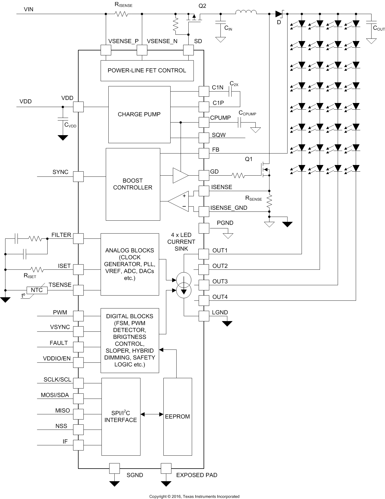
8.2 Functional Block Diagram
8.3 Feature Description
8.3.1 Clock Generation
The LP8860-Q1 has an internal 10-MHz oscillator which is used for clocking the PWM input duty cycle measurement. The 10-MHz clock is divided by two, and the 5-MHz clock is used for clocking the state machine and internal timings.
The internal 5-MHz clock can be used for generating the LED PWM output frequency directly or it can be multiplied with an internal PLL to achieve higher resolution. The higher clock frequency for the PWM generation block allows the higher resolution; however, the tradeoff is higher power consumption of the part. Clock multiplication is set with <PWM_RESOLUTION[1:0]> EEPROM bits.
8.3.1.1 LED PWM Clock Generation With VSYNC
Unsynchronized LCD line scanning and LED backlight ripple may cause a “waterfall” effect. Synchronizating LED output PWM frequency with video processor or timing controller VSYNC/HSYNC signal can reduce this effect.
The PLL can be used for generating required PWM generation clock from the VSYNC signal. This ensures that the LED output PWM remains synchronized to the VSYNC signal, and there is no clock variation between the LCD display video update and the LED backlight output frequency. If PWM_COUNTER_RESET = 1, the VSYNC signal rising edge restartsthe PWM generation, ensuring there is no clock drifting. The slow divider is intended for LED PWM frequency synchronization with an external VSYNC. An external filter connected to the FILTER pin must be used only if a slow divider is enabled — otherwise the LP8860-Q1 uses internal compensation.
The ƒOUT of the PLL must be chosen in the 5-MHz to 40-MHz range. If VSYNC is enabled, the signal must be active before VDDIO/EN is set high and present whenever VDDIO/EN is high.
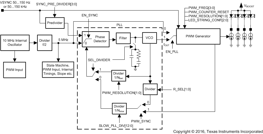 Figure 9. PLL Clock Generation
8.3.1.2 LED PWM Frequency and Resolution
LED output PWM frequency is selected with <PWM_FREQ[3:0]> EEPROM register when using a 5-MHz internal oscillator for generating PWM output. <LED_STRING_CONF[2:0]> bits define phase shift between LED outputs as described later. <PWM_RESOLUTION[1:0]> EEPROM bits select the PLL output frequency and hence the LED PWM resolution. PWM frequencies with <EN_SYNC> = 0 are listed in Table 1.
NOTE
If the VSYNC signal is used for generating PWM output frequency, it affects all clock frequencies, as well as the LED PWM output frequency. The EEPROM Bit Explanations section explains how all the dividers affect the output clocks.
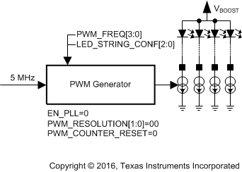 Figure 10. PWM Clocking With Internal Oscillator
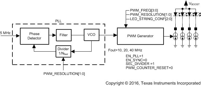 Figure 11. PWM Clocking With PLL, Internal Oscillator as Reference
Table 1. Output PWM Frequency and Resolution With Internal Oscillator
| 00 OSC = 5 MHz |
01 OSC = 10 MHz |
10 OSC = 20 MHz |
11 OSC = 40 MHz |
||
|---|---|---|---|---|---|
| PWM_FREQ[3:0] | PWM_RESOLUTION[1:0] PWM FREQUENCY (Hz) |
RESOLUTION (bit) | |||
| 1111 | 39063 | 7 | 8 | 9 | 10 |
| 1110 | 34180 | 7 | 8 | 9 | 10 |
| 1101 | 30518 | 7 | 8 | 9 | 10 |
| 1100 | 29297 | 7 | 8 | 9 | 10 |
| 1011 | 28076 | 7 | 8 | 9 | 10 |
| 1010 | 26855 | 7 | 8 | 9 | 10 |
| 1001 | 25635 | 7 | 8 | 9 | 10 |
| 1000 | 24412 | 7 | 8 | 9 | 10 |
| 0111 | 23192 | 7 | 8 | 9 | 10 |
| 0110 | 21973 | 7 | 8 | 9 | 10 |
| 0101 | 20752 | 7 | 8 | 9 | 10 |
| 0100 | 19531 | 8 | 9 | 10 | 11 |
| 0011 | 17090 | 8 | 9 | 10 | 11 |
| 0010 | 13428 | 8 | 9 | 10 | 11 |
| 0001 | 9766 | 9 | 10 | 11 | 12 |
| 0000 | 4883 | 10 | 11 | 12 | 13 |
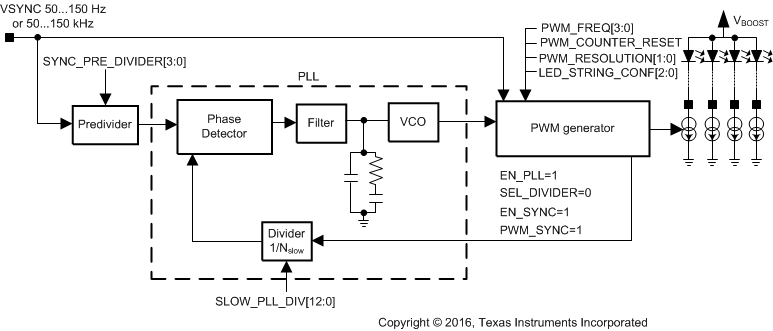 Figure 12. PWM Synchronization With External VSYNC Input
PWM clock frequencies with different <SEL_DIVIDER>, <EN_PLL>, and <EN_SYNC> combinations are listed in Table 2.
Table 2. PLL Clock and LED PWM Frequency
| PWM_SYNC | SEL_DIVIDER | EN_PLL | EN_SYNC | PLL CLOCK | PWM FREQUENCY |
|---|---|---|---|---|---|
| 0 | X | 0 | 0 | 5 MHz | See Table 1 |
| 0 | 1 | 1 | 0 | 5, 10, 20, 40 MHz | See Table 1 |
| 0 | 0 | 1 | 1 | SYNC × R_SEL[1:0] × SLOW_PLL_DIV[12:0]/ SYNC_PRE_DIV[3:0] |
PLL clock / GEN_DIV |
| 1 | 0 | 1 | 1 | SYNC × GEN_DIV × SLOW_PLL_DIV[12:0]/ SYNC_PRE_DIV[3:0] |
PLL clock / GEN_DIV |
GEN_DIV coefficients and resolution (bit) are listed on Table 3.
Table 3. GEN_DIV Coefficients and Resolution
| PWM_RESOLUTION[1:0] | ||||||||||||
|---|---|---|---|---|---|---|---|---|---|---|---|---|
| 00 | 01 | 10 | 11 | |||||||||
| PWM_ FREQ[3:0] |
STEP | GEN_DIV | RES (bits) |
STEP | GEN_DIV | RES (bits) |
STEP | GEN_DIV | RES (bits) |
STEP | GEN_DIV | RES (bits) |
| 0000 | 64 | 1024.00 | 10 | 32 | 2048.00 | 11 | 16 | 4096.00 | 12 | 8 | 8192.00 | 13 |
| 0001 | 128 | 512.00 | 9 | 64 | 1024.00 | 10 | 32 | 2048.00 | 11 | 16 | 4096.00 | 12 |
| 0010 | 176 | 372.36 | 8 | 88 | 744.73 | 9 | 44 | 1489.45 | 10 | 22 | 2978.91 | 11 |
| 0011 | 224 | 292.57 | 8 | 112 | 585.14 | 9 | 56 | 1170.29 | 10 | 28 | 2340.57 | 11 |
| 0100 | 256 | 256.00 | 8 | 128 | 512.00 | 9 | 64 | 1024.00 | 10 | 32 | 2048.00 | 11 |
| 0101 | 272 | 240.94 | 7 | 136 | 481.88 | 8 | 68 | 963.76 | 9 | 34 | 1927.53 | 10 |
| 0110 | 288 | 227.56 | 7 | 144 | 455.11 | 8 | 72 | 910.22 | 9 | 36 | 1820.44 | 10 |
| 0111 | 304 | 215.58 | 7 | 152 | 431.16 | 8 | 76 | 862.32 | 9 | 38 | 1724.63 | 10 |
| 1000 | 320 | 204.80 | 7 | 160 | 409.60 | 8 | 80 | 819.20 | 9 | 40 | 1638.40 | 10 |
| 1001 | 336 | 195.05 | 7 | 168 | 390.10 | 8 | 84 | 780.19 | 9 | 42 | 1560.38 | 10 |
| 1010 | 352 | 186.18 | 7 | 176 | 372.36 | 8 | 88 | 744.73 | 9 | 44 | 1489.45 | 10 |
| 1011 | 368 | 178.09 | 7 | 184 | 356.17 | 8 | 92 | 712.35 | 9 | 46 | 1424.70 | 10 |
| 1100 | 384 | 170.67 | 7 | 192 | 341.33 | 8 | 96 | 682.67 | 9 | 48 | 1365.33 | 10 |
| 1101 | 400 | 163.84 | 7 | 200 | 327.68 | 8 | 100 | 655.36 | 9 | 50 | 1310.72 | 10 |
| 1110 | 448 | 146.29 | 7 | 224 | 292.57 | 8 | 112 | 585.14 | 9 | 56 | 1170.29 | 10 |
| 1111 | 512 | 128.00 | 7 | 256 | 256.00 | 8 | 128 | 512.00 | 9 | 64 | 1024.00 | 10 |
Dithering allows increased resolution and smaller average steps size. Dithering can be programmed with EEPROM bits <DITHER[2:0]> 0 to 4 bits. Figure 13 shows 1-bit dithering. For 3-bit dithering, every 8th pulse is made 1 LSB longer to increase the average value by 1/8th. Dither is available in steady state condition when <EN_STEADY_DITHER> is high, otherwise during slope only.
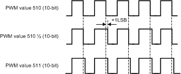 Figure 13. Example of the Dithering, 1-Bit Dither, 10-Bit Resolution
8.3.2 Brightness Control (Display Mode)
The LP8860-Q1 LED outputs can be configured to display or cluster mode. The following sections describe display mode options. Cluster mode is a special mode with individually controlled LED outputs. See Cluster Mode section for details.
The LP8860-Q1 controls the brightness of the display with conventional PWM or with Hybrid PWM and Current dimming. Brightness control is received either from PWM input pin or from I2C/SPI register bits. The brightness source is selected with <BRT_MODE[1:0]> bits as follows:
Table 4. Brightness Control Selection
| BRT_MODE[1:0] | BRIGHTNESS CONTROL |
|---|---|
| 00 | PWM input duty cycle |
| 01 | PWM input duty cycle x Brightness register |
| 10 | Brightness register |
| 11 | PWM direct control (PWM in = PWM out) |
8.3.2.1 PWM Input Duty Cycle Based Control
In this mode the LED brightness is controlled by the input PWM duty cycle. The PWM detector block measures the duty cycle in the PWM pin and uses this 16-bit value to control the duty cycle of the LED output PWM. Input PWM period is measured from rising edge to the next rising edge.
The ratio of input PWM frequency and 10-MHz sampling clock defines resolution reachable with external PWM.
PWM input block timeout is 24 ms after the last rising edge; it must be taken into account for 0% and 100% brightness setting. For setting 100% brightness, a high-level PWM input signal must last at least 24 ms. The minimum on and off time for the PWM input signal is 400 ns.
8.3.2.2 Brightness Register Control
With brightness register control the LED output PWM is controlled with 16-bit resolution <DISP_CL1_BRT[15:0]> register bits.
8.3.2.3 PWM Input Duty × Brightness Register
In this mode the PWM input duty cycle value is multiplied with the 16-bit <DISP_CL1_BRT[15:0]> register value to achieve the LED output PWM.
8.3.2.4 PWM-Input Direct Control
With PWM-input direct control the output PWM directly follows the input PWM frequency and duty cycle. Due to the internal logic structure the input is clocked with the 5-MHz clock or the PLL clock (if it is enabled). The output PWM delay can be 5 to 6 clock cycles from input PWM.
In the direct control mode several of the advanced features are not available: Phase Shift PWM (PSPWM), brightness slope, dither, Hybrid PWM and Current dimming, and LED current limitation with external NTC.
Dimming ratio can be calculated as the ratio between the brightness PWM input signal and sampling clock (5-MHz or PLL clock) frequencies. In direct mode PWM duty cycle must be less than 100%. Boost adaptive mode turns off at 100% duty cycle.
8.3.2.5 Brightness Slope
Sloper makes the smooth transition from one brightness value to another. Slope time can be programmed with EEPROM bits <PWM_SLOPE[2:0]> from 0 to 511 ms. Slope time is used for sloping up and down. Advanced slope makes brightness changes smooth for eye.
Table 5. Slope Time
| PWM_SLOPE[2:0] | SLOPE TIME |
|---|---|
| 000 | disabled |
| 001 | 1 ms |
| 010 | 2 ms |
| 011 | 52 ms |
| 100 | 105 ms |
| 101 | 210 ms |
| 110 | 315 ms |
| 111 | 511 ms |
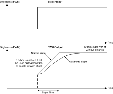 Figure 14. Sloper Operation
8.3.2.6 LED Dimming Methods
In additional to conventional PWM dimming control the LP8860-Q1 supports Hybrid PWM and Current dimming. Hybrid dimming combines the PWM and current dimming methods. PWM dimming operates with a lower range of light, and linear current dimming is used with higher brightness values. If the <EN_PWM_I EEPROM> bit is set to 1, the system enables hybrid dimming. Principles of PWM dimming and Hybrid PWM and Current dimming are illustrated by Figure 15. Only 25% switch points and slope gain = 1 are shown for simplicity.
 Figure 15. Principles of PWM Dimming and Hybrid PWM and Current Dimming
LED forward voltage increases and efficiency declines when forward current is increased. Use of constant current with PWM dimming at lower brightness and current dimming at greater brightness (instead of PWM dimming at full brightness range), yields better optical efficiency and resolution especially at lower brightness values. The optimum switch point between PWM and current dimming modes and current slope depend on the LED type.
PWM control ranges from 12.5% to 50% and the current slope can be selected using <GAIN_CTRL[2:0]> and <I_SLOPE[2:0]> EEPROM bits, respectively (see Table 6 and Table 7).
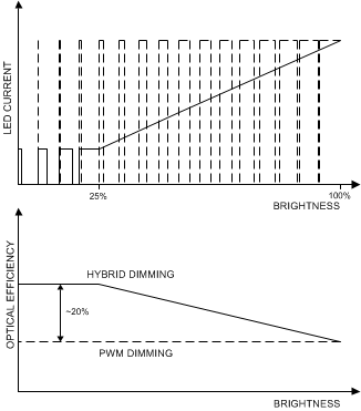 Figure 16. Optical Efficiency Improvement With PWM and Current Dimming
Table 6. Gain Control Selections
| GAIN_CTRL[2:0] | SWITCH POINT FROM PWM TO CURRENT DIMMING |
|---|---|
| 000 | 50.0% |
| 001 | 40.6% |
| 010 | 31.3% |
| 011 | 25.0% |
| 100 | 21.9% |
| 101 | 18.8% |
| 110 | 15.6% |
| 111 | 12.5% |
Table 7. Current Slope Control Selections
| I_SLOPE[2:0] | SLOPE GAIN |
|---|---|
| 000 | 1.000 |
| 001 | 1.023 |
| 010 | 1.047 |
| 011 | 1.070 |
| 100 | 1.094 |
| 101 | 1.117 |
| 110 | 1.141 |
| 111 | 1.164 |
The current setting for DISP_CL1_CURRENT[11:0] in Hybrid PWM and Current dimming mode can be defined by the following formula (assuming individual LED sink current correction DRV_OUTx_CORR[3:0] is 0%):

Example of calculation for Hybrid PWM and Current dimming mode, 100-mA maximum output current:
| Target maximum current 100 mA | IDISP_CL1_CURRENT = 100 – 100 × 1 × ((100 – 25) / 100) = 25 mA |
| Maximum scale 100 mA (DRV_LED_CURRENT_SCALE[2:0]=101) | |
| Slope = 1.000 (I_SLOPE[2:0]=000) | |
| Switch point = 25% (GAIN_CTRL[2:0]=011) |
Example of calculation for Hybrid PWM and Current dimming mode, 23-mA maximum output current:
| Target maximum current 23 mA | IDISP_CL1_CURRENT = 23 – 25 × 1.094 × ((100 – 25) / 100) = 2.49 mA |
| Maximum scale 25 mA (DRV_LED_CURRENT_SCALE[2:0]=000) | |
| Slope = 1.094 (I_SLOPE[2:0]=100) | |
| Switch point = 25% (GAIN_CTRL[2:0]=011) |
NOTE
- Formula is only approximation for the actual value.
- DISP_CL1_CURRENT[11:0] value must be chosen to avoid current saturation before 100% brightness is achieved.
8.3.2.7 PWM Calculation Data Flow for Display Mode
Figure 17 shows the PWM calculation data flow for display mode. In PWM direct control mode most of the blocks are bypassed, and this flow chart does not apply.
 Figure 17. PWM Data Flow Calculation
Table 8. PWM Calculation Blocks
| BLOCK NAME | DESCRIPTION |
|---|---|
| PWM detector | PWM detector block measures the duty cycle of the input PWM signal. Resolution depends on the input signal frequency. Hysteresis selection sets the minimum allowable change to the input. Smaller changes are ignored. |
| Brightness register | 16-bit register for brightness setting <DISP_CL1_BRT[15:0]> |
| Brightness mode control | Brightness control block gets 16-bit value from the PWM detector, and also 16-bit value from the brightness register <DISP_CL1_BRT[15:0]>. <BRT_MODE[1:0]> selects whether to use PWM input duty cycle value, the brightness register value or multiplication. |
| Temperature regulator | Temperature regulator reduces LED PWM duty cycle depending on internal and external temperature sensor. See LED Current Dimming With Internal Temperature Sensor and LED Current Limitation With External NTC Sensor for details |
| External temperature sensor | External NTC temperature sensor |
| Internal temperature sensor | Internal die temperature sensor |
| Sloper | Sloper makes the smooth transition from one brightness value to another. Slope time can be adjusted from 0 ms to 511 ms with <PWM_SLOPE[2:0]> EEPROM bits. |
| Advanced sloper | Advanced slope makes brightness changes smoother for eye; see Brightness Slope for details |
| PWM and Current Control | Hybrid PWM and Current dimming improves the optical efficiency of the LEDs by using PWM control with lower brightness values and current control with greater values. <EN_PWM_I> EEPROM bit enables Hybrid PWM and Current control. PWM dimming range can be set 12.5 to 50% of the brightness range with <GAIN_CTRL[2:0]> EEPROM bits. Current slope can be adjusted by using the <I_SLOPE[2:0]> EEPROM bits. See LED Dimming Methods for details |
| Dither | With dithering the output resolution can be further increased. This way the brightness change steps are not visible to eye. The amount of dithering is 0 to 4 bits, and is selected with <DITHER[2:0]> EEPROM bits. |
| PWM comparator | PWM comparator compares the PWM counter output to the value received from the dither block. Output of the PWM comparator directly controls the LED current sinks. If Phase Shift PWM (PSPWM) mode is used, the PWM counter values for each LED output are modified by summing an offset value to create different phases. |
| PWM counter | Overflowing 16-bit PWM counter creates new PWM cycle. Step for incrementation is defined by <PWM_FREQ[3:0]> and <PWM_RESOLUTION[1:0]> bits, see Table 3. |
8.3.3 LED Output Modes and Phase Shift PWM (PSPWM) Scheme
The PSPWM scheme allows delaying the time when each LED output is active. When the LED outputs are not activated simultaneously, the peak load current from the boost output is greatly decreased. This reduces the ripple seen on the boost output and allows smaller output capacitors. Reduced ripple also reduces the output ceramic capacitor audible ringing. The PSPWM scheme also increases the load frequency seen on boost output up to 4 times, therefore transferring possible audible noise to a frequency above human hearing range. In addition, “optical ripple” through the LCD panel is reduced helping in waterfall noise reduction.
Figure 18 shows the available LED output modes. The number of LED outputs used can be one to four; outputs can be tied together to increase current for one string or all four strings can be independently controlled in the cluster mode.
In <LED_STRING_CONF[2:0]> = 000 the phase difference between channels is 90 degrees. This mode is intended for application in Figure 53. When <LED_STRING_CONF[2:0] > = 001 the phase difference between 3 channels in display mode is 120 degrees. This mode is intended for application shown in Figure 63. When <LED_STRING_CONF[2:0]> = 010 the phase difference between 2 channels in display mode is 180 degrees, channels 3 and 4 in cluster mode, intended for application illustrated by Figure 60. LED strings not used in Display mode can be used for Cluster mode, or not used. When <LED_STRING_CONF[2:0]> = 111 all strings are in cluster mode.
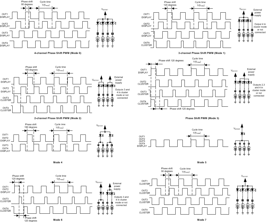 Figure 18. Phase Shift Modes
Table 9. Description of the LED Output Modes
| MODE | LED_STRING_CONF[2:0] | DESCRIPTION |
|---|---|---|
| 0 | 000 | 4 separate LED strings with 90° phase shift |
| 1 | 001 | 3 separate LED strings with 120° phase shift (String 4 in cluster mode or not used) |
| 2 | 010 | 2 separate LED strings with 180° phase shift (Strings 3 and 4 in cluster mode or not used) |
| 3 | 011 | 1 LED string. (Strings 2,3 and 4 in cluster mode or not used) |
| 4 | 100 | 2 LED strings (1+2, 3+4) with 180° phase shift. Strings with same phase can be connected together. |
| 5 | 101 | 1 LED string (1+2+3+4). All strings with same phase (can be tied together). |
| 6 | 110 | 1 LED string (1+2). 1st and 2nd strings tied with same phase, strings 3 and 4 are in cluster mode or not used |
| 7 | 111 | All strings are used in cluster mode with 90° phase shift |
Table 10. Output Mode Configuration
| LED_STRING_CONF[2:0] | 000 | 001 | 010 | 011 | 100 | 101 | 110 | 111 | ||||||||
|---|---|---|---|---|---|---|---|---|---|---|---|---|---|---|---|---|
| SETUP | No. of Displ. Strings | No. of Cluster Strings | No. of Displ. Strings | No. of Cluster Strings | No. of Displ. Strings | No. of Cluster Strings | No. of Displ. Strings | No. of Cluster Strings | No. of Displ. Strings | No. of Cluster Strings | No. of Displ. Strings | No. of Cluster Strings | No. of Displ. Strings | No. of Cluster Strings | No. of Displ. Strings | No. of Cluster Strings |
| 4 | 0 | 3 | 1 | 2 | 1+1 | 1 | 1+1+1 | 2+2 | 0 | same phase/
4 tied |
0 | same phase/
2 tied |
1+1 | 0 | 1+1+1+1 | |
| Adaptive voltage control | Y | Y | N | Y | N | Y | N | Y | Y | Y | N | N | ||||
| FAULT DETECTION | ||||||||||||||||
| Open LED string | Y | Y | Y | Y | Y | Y | Y | Y | Y | Y | Y | Y | ||||
| Short LED string | Y | Y | Y | Y | Y | N | Y | Y | Y/N | Y/N | Y | Y | ||||
| OPTIONS | ||||||||||||||||
| Sloper | Y | Y | N | Y | N | Y | N | Y | Y | Y | N | N | ||||
| Dithering | ||||||||||||||||
| Int. temp. current dimming | ||||||||||||||||
| Ext. temp. current limit | ||||||||||||||||
| Ext. temp. current dimming | Y | Y | Y | Y | Y | |||||||||||
| Brightness modes | All | All | Reg. only | All | Reg. only | All | Reg. only | All | All | All | Reg. only | Reg. only | ||||
| PMW dimming | Y | Y | Y | Y | Y | Y | Y | Y | Y | Y | Y | Y | ||||
| Hybrid PWM and Current Dimming | N | N | N | N | N | |||||||||||
| LED OUTPUT PARAMETERS (PLL Frequency 40 MHz) | ||||||||||||||||
| ƒLED PWM min | 4.9 kHz | 4.9 kHz | 4.9 kHz | 4.9 kHz | 4.9 kHz | |||||||||||
| Resolution at min ƒLED PWM | 13 | 13 | 13 | 13 | 13 | |||||||||||
| fLED PWM max | 39 kHz | 39 kHz | 39 kHz | 39 kHz | 4.9 kHz | |||||||||||
| Resolution at max ƒLED PWM | 10 | 10 | 10 | 10 | 13 | |||||||||||
| Additional Dither for Display | 4 | 4 | N | 4 | N | 4 | N | 4 | 4 | 4 | N | N | ||||
| LED OUTPUT PARAMETERS (PLL Frequency 5 MHz/off | ||||||||||||||||
| fLED PWM min | 4.9 kHz | 4.9 kHz | 4.9 kHz | 4.9 kHz | 610 Hz | |||||||||||
| Resolution at min ƒLED PWM | 10 | 10 | 10 | 10 | 13 | |||||||||||
| ƒLED PWM Max | 39 kHz | 39 kHz | 39 kHz | 39 kHz | 610 Hz | |||||||||||
| Resolution at max ƒLED PWM | 7 | 7 | 7 | 13 | ||||||||||||
| Additional bits with dither | 4 | 4 | N | 4 | N | 4 | N | 4 | 4 | 4 | N | N | ||||
8.3.4 LED Current Setting
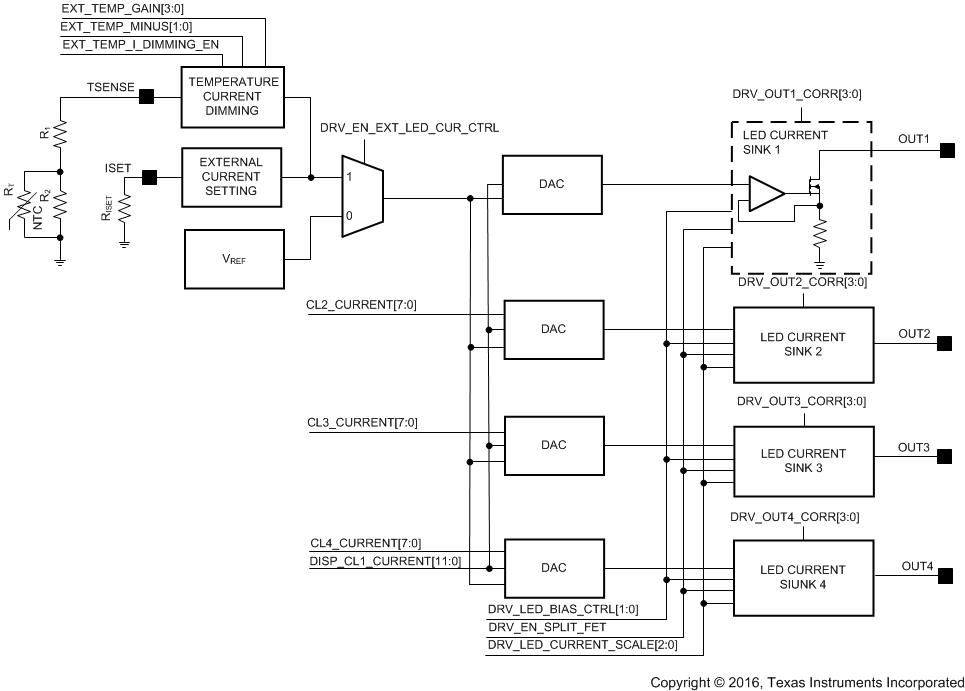 Figure 19. LED Current Setting
The output LED current can be set by a register. Maximum output LED current can be set by an external resistor when that option is enabled. For strings in cluster mode current for every LED output can be set independently.
The maximum current for the LED outputs in display mode are controlled with <DISP_CL1_CURRENT [11:0]> bits. Current for the outputs in the cluster mode are controlled separately by the register bits <DISP_CL1_CURRENT[11:0]>, <CL2_CURRENT[7:0]>, <CL3_CURRENT[7:0]>, and <CL4_CURRENT[7:0]> respectively. In the display mode resolution for current control is 12 bits. In the cluster mode resolution is 8 bits for all outputs except OUT1. For OUT1 maximum current resolution is always 12 bits.
Additionally, current for every output current can be scaled with <DRV_LED_CURRENT_SCALE[2:0]> bits (see Table 11) and can be corrected by <DRV_OUTx_CORR[3:0]> EEPROM bits. The adjustment range is shown in Table 12 Maximum current settings are effective for display and cluster modes.
Table 11. LED Current Scaling
| DRV_LED_CURRENT_SCALE[2:0] | MAXIMUM CURRENT |
|---|---|
| 000 | 25 mA |
| 001 | 30 mA |
| 010 | 50 mA |
| 011 | 60 mA |
| 100 | 80 mA |
| 101 | 100 mA |
| 110 | 120 mA |
| 111 | 150 mA |
When maximum current is controlled by anexternal resistor RISET (<DRV_EN_EXT_LED_CUR_CTRL>=1), current for outputs in display mode or for OUT1 in cluster mode can be calculated as follows:

Where VBG = 1.2 V.
space
For example, if <DISP_CL1_CURRENT[11:0]> is 0xFFF, <DRV_LED_CURRENT_SCALE[0:2]> is 111, and a 24-kΩ RISET resistor is used, then the LED maximum current is 150 mA.
When current control with external resistor is disabled (<DRV_EN_EXT_LED_CUR_CTRL>=0) LED current for outputs in display mode or for OUT1 in cluster mode can be calculated as follow:

When maximum current control with external resistor is enabled, LED current for OUT2…OUT4 outputs in cluster mode is defined as:

Otherwise, when current control with external resistor is disabled:

Correction value is defined by <DRV_OUTx_CORR[3:0]> shown in Table 12:
Table 12. Individual Current Correction
| DRV_OUTx_CORR[3:0] | CORRECTION |
|---|---|
| 0000 | 6.50% |
| 0001 | 5.60% |
| 0010 | 4.70% |
| 0011 | 3.70% |
| 0100 | 2.80% |
| 0101 | 1.90% |
| 0110 | 0.90% |
| 0111 | 0.00% |
| 1000 | –0.9% |
| 1001 | –1.90% |
| 1010 | –2.80% |
| 1011 | –3.70% |
| 1100 | –4.70% |
| 1101 | –5.60% |
| 1110 | –6.50% |
| 1111 | –7.40% |
NOTE
Formulas are only approximation for the actual current.
The <DISP_CL1_CURRENT[11:0]> register is initialized during start-up by the <LED_CURRENT_CTRL[11:0]> EEPROM bits. <DRV_LED_CURRENT_SCALE[2:0]> are initialized by the <DRV_LED_CURRENT_SCALE[2:0]> EEPROM bits. Cluster mode current registers for outputs OUT2 and OUT3 are initialized by 0 during power on reset.
Current register value must be not written to 0 if brightness is not zero – it may cause LED faults and adaptive voltage control instability.
8.3.5 Cluster Mode
Cluster is a simplified mode which allows independent current and PWM control for every string in cluster mode. In this mode brightness control is limited to conventional PWM through the SPI/I2C brightness registers. The PWM input pin, Hybrid PWM and Current dimming mode, slope control, or dither are not available. Brightness for different LED strings depends on <DISP_CL1_BRT[15:0]>, <CL2_BRT[12:0]>, <CL3_BRT[12:0]> and <CL4_BRT[12:0]> registers. If OUT1 is in cluster mode, only 13 MSB are used. If all LED outputs are in the cluster mode, LED output PWM resolution is always 13 bits, and frequency depends on <PWM_RESOLUTION[1:0]> bits (see Table 13). If one or more of the LED outputs is in display mode, frequency, and resolution for strings in the cluster mode is the same as for strings in the display mode (see Table 1).
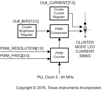 Figure 20. Cluster Mode Block Diagram
Table 13. Output PWM Frequency for Mode 7 (All Strings in Cluster Mode)
| PWM_RESOLUTION[1:0] | 00 | 01 | 10 | 11 |
|---|---|---|---|---|
| OSC frequency (MHz) | 5 | 10 | 20 | 40 |
| ƒLED PWM (Hz) | 610 | 1221 | 2442 | 4883 |
When the LP8860-Q1 is set in cluster mode, fault protection functionality is limited. Headroom for LED strings must be between the high-voltage comparator level <DRV_LED_FAULT_THR[1:0]> and low-voltage comparator level <DRV_HEADR[2:0]> (which depend upon saturation voltage); otherwise a fault is generated.
Adaptive boost control does not follow strings in cluster mode. Display mode strings and cluster mode strings must not be connected to the same boost. When LED strings in display and cluster modes are connected to the same boost, LED open or short faults may be generated if the LED forward-voltage mismatch is too high.
If all LED outputs are in cluster mode, boost output voltage is fixed and must be set by EEPROM <BOOST_INITIAL_VOLTAGE[5:0]> bits to a value high enough to ensure correct LED string operation in all conditions.
<EN_CL_LED_FAULT>=0 disables cluster LED fault detection, even if all LED strings are in the cluster mode. The current de-rating (based on the internal temperature sensor) and LED current limitation (based on external temperature sensor) are not functional in this mode, and analog current dimming based on the external sensor functionality is limited (LED shutdown for high temperature is not operational).
8.3.6 Boost Controller
The LP8860-Q1 boost controller generates a 16-V to 48-V supply voltage for the LEDs. Output voltage can be increased by an external resistive voltage divider connected to the FB pin, but voltage lower than 16 V is not supported.
The output voltage can be controlled either with EEPROM register bits <BOOST_INITIAL_VOLTAGE[5:0]>, or automatic adaptive boost control can be used. During start-up the output voltage is ramped to default start-up voltage <BOOST_INITIAL_VOLTAGE[5:0]> where it then adapts to the required voltage based on LED output headroom voltage (if adaptive mode has been enabled in EEPROM). Initial voltage for adaptive voltage control mode must be higher than LED string voltage — otherwise the system may generate a boost overvoltage fault during VDDIO/EN pin toggling if the output boost capacitor is not discharged below the initial voltage before the next boost start-up. A different option is to set <MASK_BOOST_OVP_STATUS> bit high to prevent a boost overvoltage fault.
The converter is a magnetic switching PWM mode DC-DC converter with a current limit. The topology of the magnetic boost converter is called Current Programmed Mode (CPM) control, where the inductor current is measured and controlled with the feedback. Switching frequency is selectable from 100 kHz and 2.2 MHz with EEPROM bits <BOOST_FREQ_SEL[2:0]>. In most cases lower frequency has the highest system efficiency.
In adaptive mode the boost output voltage is adjusted automatically based on LED current sink headroom voltage. Boost output voltage control step size is, in this case, 125 mV to ensure as small as possible current sink headroom and high efficiency. The adaptive mode is enabled with the <EN_ADAP EEPROM> bit. If boost is started with adaptive mode enabled, then the initial boost output voltage value is defined with the <BOOST_INITIAL_VOLTAGE[5:0]> EEPROM register bits in order to eliminate long output voltage iteration time when boost is started after VDDIO/EN toggling or power-on reset.
Boost can be clocked by an external SYNC signal (100 kHz to 2.2 MHz); minimum pulse length for the signal is 200 ns. If an external SYNC disappears, boost uses internal frequency defined by <BOOST_FREQ_SEL[2:0]> EEPROM bits. The boost frequency with external SYNC and EEPROM bits-defined frequency need to be close to each other; maximum frequency mismatch is ±25%. The boost controller has optional spread-spectrum switching operation (±3% from central frequency, 1.875-kHz modulation frequency) which reduces spectrum spikes around the switching frequency and its harmonic frequencies.
Further EMI reduction can be achieved by limiting the rise and fall times of the FET with an additional external resistor on the GD pin.
The boost gate driver is powered directly from VDD voltage or from the charge pump which multiplies VDD voltage by 2. If the charge pump is disabled, the VDD and CPUMP pins must be tied together.
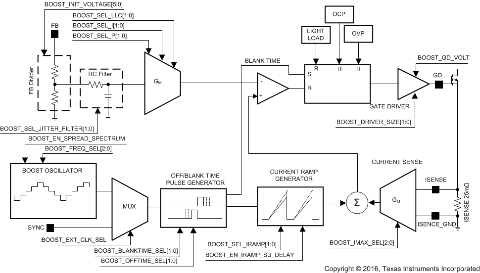 Figure 21. Boost Converter Topology
8.3.7 Charge Pump
The boost switch FET gate driver is powered typically from VDD voltage. When the VDD voltage is not high enough to drive the boost FET gate, the charge pump can be used to increase gate-driver voltage.
The charge pump effectively doubles the VDD voltage for gate driver. Maximum DC output current is 50 mA. Boost driver voltage selection bit BOOST_GD_VOLT must be set to 1 before enabling the charge pump. If VDD voltage is 5 V, the charge pump is not typically needed. In this case, a flying capacitor is not necessary, and the charge pump output CPUMP pin must be connected to the VDD input pin.
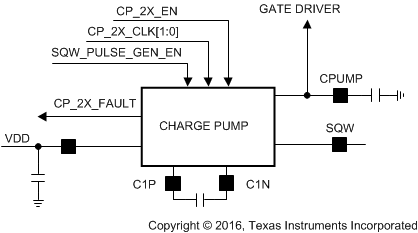 Figure 22. Charge Pump
Table 14. Charge Pump Clock Frequency
| CP_2X_CLK | FREQUENCY (kHz) |
|---|---|
| 00 | 104 |
| 01 | 208 |
| 10 | 417 |
| 11 | 833 |
Square-waveform (SQW) output provides a 100-kHz square wave signal (1 mA max) with amplitude equal to the charge pump output voltage. When the charge pump is disabled, amplitude of this voltage is equal to VDD. This signal can be used to generate low-current voltage rails; for example, a gate-reference voltage for output protective FET (Figure 61) or for using nMOSFET as power-line FET (Figure 25). Figure 23 and Figure 24 show examples of possible connections.
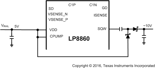 Figure 23. VRAIL Multiplied by 2
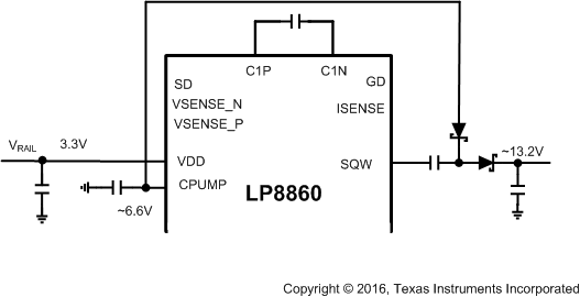 Figure 24. VRAIL Multiplied by 4
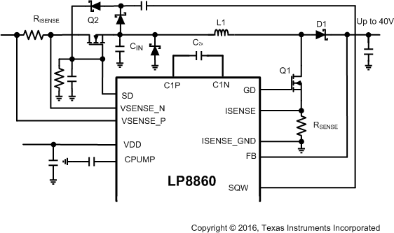 Figure 25. Using nFET for Power-Line Control
8.3.8 Powerline Control FET
The power-line FET limits peak current from the power line during start-up and allows the boost and LED strings to be disconnected during a fault condition, when device is in fault recovery state.
The power-line control block has VSENSE_P and VSENSE_N pins for sensing input current and a shutdown SD pin for driving the gate of the power-line FET. The power-line FET is opened when the LP8860-Q1 is enabled by VDDIO/EN signal and VIN is greater than VGS in steady state (when pFET is used as a power-line FET). A power-line pFET must be chosen with minimal VGS in steady state. Gate current is defined by the <PL_SD_SINK_LEVEL[1:0]> EEPROM bits.
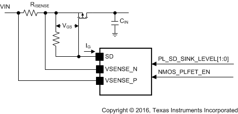 Figure 26. Power-line FET Control
During a shutdown state the LP8860-Q1 closes the power-line FET and prevents possible boost and LED leakage. Sense pins are used to detect overcurrent. Power-line FET is closed when an OCP fault occurs. A VIN OCP is indicated with PL_FET_FAULT bit. The power-line FET closes with all faults, followed by entering to a recovery state.
When it is not possible to choose a pFET with the necessary characteristics, a schematic with nFET can be used (see Charge Pump section, Figure 25); the <NMOS_PLFET_EN EEPROM> bit must be set accordingly. In this case the SD pin provides current to shut down the power-line nFET during fault condition.
8.3.9 Protection and Fault Detection Modes
The LP8860-Q1 has fault detection for LED outputs, low and high input voltage, power line overcurrent, boost overcurrent, boost overvoltage, and charge pump overload. In addition, the device has thermal shutdown and LED overtemperature protection with an external NTC thermistor.
Faults have dedicated fault flags in registers <FAULT> and <LED_FAULT>. Mask bits can be used to disable certain faults (see Table 17 for details). In addition the open-drain output pin FAULT can be used to indicate occurred fault. Writing CLEAR_FAULTS or setting the NSS pin (I2C interface mode only) high resets the fault. Setting the VDDIO/EN pin low, then high again, resets the faults as well.
8.3.9.1 LED Fault Comparators and Adaptive Boost Control
Every LED current sink has 3 comparators for adaptive boost control and fault detection. Each comparator outputs is filtered. Filter control bits <BL_COMP_FILTER_SEL [3:0]> select how many PWM generator clock cycles (5 MHz if PLL disabled or PLL clock) high/mid comparator is filtered before it is used to detect shorted LEDs and boost voltage down-scaling. Usually 1 µs is sufficient; for 5-MHz frequency it means <BL_COMP_FILTER_SEL [3:0]> = 0000b, 10 MHz = 0001b, 20 MHz = 0010b, and 40 MHz = 0011b.
Adaptive boost-control function adjusts the boost output voltage to the minimum sufficient voltage for proper LED current sink operation. The output with the highest VF LED string is detected and the boost output voltage adjusted accordingly. Current sink headroom can be adjusted with EEPROM bits <DRV_HEADR[2:0]>. Boost adaptive control voltage step size is 125 mV. Boost adaptive control operates similarly with and without PSPWM. Additionally, when faster boost response is needed in larger brightness steps, the "jump" command can be used. Jump allows increase of the boost voltage with greater steps. Jump is enabled with the <EN_JUMP> EEPROM bit. The threshold for the magnitude of brightness increase that requires use of jump can be set with the <JUMP_STEP_SIZE[1:0]> EEPROM bits. <BRIGHTNESS_JUMP_THRES[1:0]> EEPROM bits define when the jump command is activated.
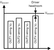 Figure 27. Boost Voltage Adaptation
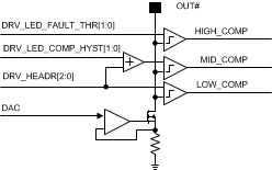 Figure 28. Output Voltage Comparators
Figure 29 shows different cases which cause boost voltage increase, decrease, or generate faults.
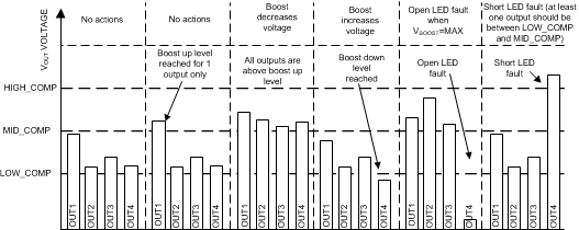 Figure 29. Protection and Boost Adaptation Algorithms
NOTE
In the Cluster mode, if voltage of one or more outputs is below LOW_COMP, it causes open LED fault detection.
8.3.9.2 LED Current Dimming With Internal Temperature Sensor
The LP8860-Q1 can prevent thermal shutdown (TSD) by reducing the average LED strings current based on die temperature.
When die temperature reaches <INT_TEMP_LIM[1:0]> EEPROM bits-defined threshold, the device automatically lowers the brightness (2.25% / ºC typical). Depending on brightness control mode either PWM duty cycle or current is used for average current reduction.
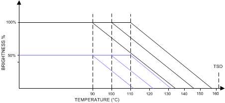 Figure 30. Thermal De-Rating Function
Example With 100% and 50% Brightness
Table 15. Thermal De-rating Function Temperature Thresholds
| INT_TEMP_LIM[1:0] | TEMPERATURE |
|---|---|
| 00 | disabled |
| 01 | 90ºC |
| 10 | 100ºC |
| 11 | 110ºC |
Table 16. Temperature ADC Output for Different Temperatures
| TEMPERATURE (°C) | DECIMAL OUTPUT VALUE OF TEMP[10:0] REGISTER | |
|---|---|---|
| VDD 3.6 (V) | VDD 5 (V) | |
| –40 | 885 | 891 |
| –35 | 901 | 907 |
| –30 | 916 | 923 |
| –25 | 932 | 939 |
| –20 | 948 | 954 |
| –15 | 964 | 970 |
| -10 | 980 | 986 |
| -5 | 994 | 1002 |
| 0 | 1010 | 1018 |
| 5 | 1026 | 1034 |
| 10 | 1041 | 1050 |
| 15 | 1057 | 1066 |
| 20 | 1073 | 1082 |
| 25 | 1089 | 1098 |
| 30 | 1105 | 1115 |
| 35 | 1121 | 1131 |
| 40 | 1137 | 1147 |
| 45 | 1154 | 1163 |
| 50 | 1170 | 1180 |
| 55 | 1186 | 1196 |
| 60 | 1202 | 1212 |
| 65 | 1219 | 1229 |
| 70 | 1235 | 1245 |
| 75 | 1252 | 1262 |
| 80 | 1268 | 1278 |
| 85 | 1285 | 1293 |
| 90 | 1301 | 1310 |
| 95 | 1318 | 1328 |
| 100 | 1332 | 1343 |
| 105 | 1349 | 1359 |
| 110 | 1365 | 1375 |
8.3.9.3 LED Current Limitation With External NTC Sensor
The <EXT_TEMP_COMP_EN> EEPROM bit enables the LED current limitation mode. The principle of current limitation is shown in Figure 31.
When LED temperature reaches <EXT_TEMP_LEVEL_LOW[3:0]> level, the device automatically tries to reduce LED average current step-by-step by 3.125% from maximum brightness value. Step time is defined by <EXT_TEMP_PERIOD[4:0]> EEPROM bits. If temperature continues to increase and reaches <EXT_TEMP_LEVEL_HIGH[3:0]> level, the device shuts down the LEDs and generates a fault condition. The LEDs are turned on automatically when the temperature is below the <EXT_TEMP_LEVEL_LOW[3:0]> level. Otherwise, if after one or more steps the temperature drops down below <EXT_TEMP_LEVEL_LOW[3:0]>, brightness increases with the same step time until it reaches the original level. The LP8860-Q1 uses PWM duty reduction to reduce LED current. The device detects external NTC resistor availability, and the <TEMP_RES_MISSING> flag is set, if the NTC sensor is missing (resistance is 2 MΩ or more).
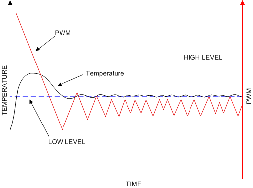 Figure 31. LED Current Limitation With NTC
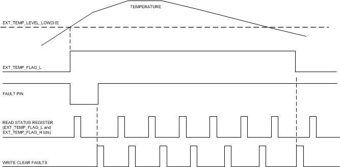 Figure 32. Timing Diagram for LED Current Limitation With NTC
8.3.9.4 LED Current Dimming With External NTC Sensor
When an external resistor for maximum current control is used, current dimming for LED current can be used also. In this case LED current can be de-rated when ambient temperature is high. This option must be enabled by <EXT_TEMP_I_DIMMING_EN> and <EXT_TEMP_COMP_EN> EEPROM bits.
Knee point and slope are defined by <EXT_TEMP_MINUS[1:0]> and <EXT_TEMP_GAIN[3:0]> EEPROM bits respectively. LED shutdown temperature is defined by <EXT_TEMP_LEVEL_HIGH[3:0]> bits. Serial and parallel resistors R1 and R2 affect the slope and knee point and can be used for the thermal curve adjustment and NTC linearization.
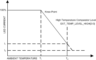 Figure 33. Current Dimming for High Ambient Temperature
 Figure 34. NTC Linearization
Figure 35 and Figure 36 show the block diagrams for current dimming.
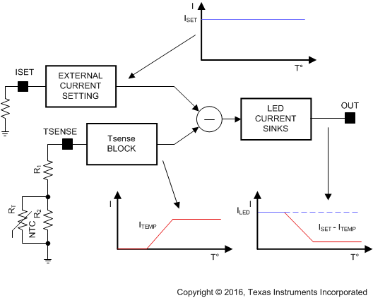 Figure 35. Temperature-Dependent NTC Current
(Subtracted from ISET Current)
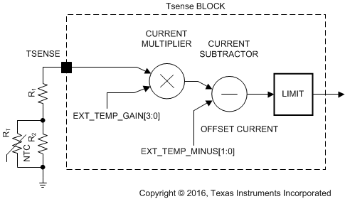 Figure 36. NTC Current Processing —
Scaling, Shift, and Limitation
Current dimming by external NTC sensor for 150-mA scale can be defined by formulas:

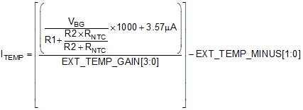
ITEMP cannot be negative; if ITEMP < 0, then ITEMP must be 0.
where
- ISET: Maximum current setting with external resistor RISET, µA
- ITEMP: Temperature compensation, µA
- RISET: External resistor, kΩ
- R1, R2: Resistors for adjustment, kΩ
- ILED: Output current per channel, mA
- EXT_TEMP_MINUS[1:0]: 1, 5, 9, 13 µA
- EXT_TEMP_GAIN[[3:0]: 50/n, n = 16 to 1
- VBG: 1.2 V
8.3.9.5 Protection Feature and Fault Summary
Table 17 summarizes protection features and related faults.
Table 17. Overview of the Fault/Protection Schemes
| FAULT/PROTECTION | FAULT NAME | THRESHOLD | ACTION(1)(2) | MASK(4) | FAULT CLEARING(3)(5) | |
|---|---|---|---|---|---|---|
| Input overvoltage protection | VIN_OVP | OVP_LEVEL[1:0] (V) | VIN overvoltage monitored from soft start. Fault causes entry to FAULT_RECOVERY state. If device is restarted successfully with recovery timer, the fault register bit is not automatically cleared. FAULT pin is pulled low. |
MASK_OVP_FSM Masks fault recovery, but not status and fault pin operations |
Fault bit and FAULT pin: 1. POR or VDDIO/EN 2. Writing CLEAR_FAULTS bit or toggling NSS pin |
|
| 00 | OFF | |||||
| 01 | 7 | |||||
| 10 | 11 | |||||
| 11 | 22.5 | |||||
| Input undervoltage protection | VIN_UVLO | UVLO_LEVEL[1:0] (V) | VIN undervoltage monitored from soft start. Fault causes entry to FAULT_RECOVERY state. If device is restarted successfully with recovery timer, the fault register bit is not automatically cleared. FAULT pin is pulled low. |
MASK_VIN_UVLO Masks fault recovery, status and fault pin operations |
Fault bit and FAULT pin: 1.POR or VDDIO/EN 2. Writing CLEAR_FAULTS bit or toggling NSS pin |
|
| 00 | OFF | |||||
| 01 | 3 | |||||
| 10 | 5 | |||||
| 11 | 8 | |||||
| VDD undervoltage protection | VDD_UVLO | VDD_UVLO_LEVEL Threshold (V) |
Device enters STANDBY state. Recovers when fault disappears. All registers are cleared or reloaded from EEPROM (if defined) with exception registers 0x00, 0x01, 0x04…0x0C. After recovery LP8860-Q1 provides the same brightness as before fault detection, if DISP_CL1_CURRENT[11:0] context stays same as LED_CURRENT_CTRL[11:0] EEPROM setting. If VDD voltage goes below POR level, registers 0x00, 0x01, 0x04…0x0C are cleared. This fault does not have any flags and doesn’t generate FAULT. Voltage hysteresis is 50 mV (typical). |
|||
| 0 | 2.5 | |||||
| 1 | 3 | |||||
| Boost overcurrent protection | BOOST_OCP | VBOOST longer than 110 ms 5 V (typical) below set value. Set value is voltage value defined by logic during adaptation in adaptive mode or initial boost voltage setting in manual mode. |
Fault monitoring started from boost start. Fault causes entry to FAULT_RECOVERY state. If device is restarted successfully with recovery timer, the fault register bit is not automatically cleared. FAULT pin is pulled low. |
MASK_BOOST_OCP_ FSM Masks fault recovery, but not status and fault pin operations |
Fault bit and FAULT pin: 1. POR or VDDIO/EN 2. Writing CLEAR_FAULTS bit or toggling NSS pin |
|
| Boost overvoltage protection | BOOST_OVP | VBOOST voltage 1.6 V (typical) above set value Set value is voltage value defined by logic during adaptation in adaptive mode or initial boost voltage setting in manual mode. |
Boost OVP fault monitored during normal operation FAULT pin is pulled low. |
MASK_BOOST_OVP_ STATUS | Fault bit and FAULT pin: 1. POR or VDDIO/EN 2. Writing CLEAR_FAULTS bit or toggling NSS pin |
|
| Input voltage overcurrent protection | PL_FET_FAULT | PL_SD_LEVEL[1:0] (A) | Fault is detected with 2 methods: 1. Detects overcurrent from soft start by measuring RISENSE voltage. 2. Detects FB voltage at the end of soft start. If voltage is below 1.2 V, fault is detected. Fault causes entry to FAULT_RECOVERY state. If device is restarted successfully with recovery timer, the fault register bit is not automatically cleared. FAULT pin is pulled low. |
Fault bit and FAULT pin: 1. POR or VDDIO/EN 2. Writing CLEAR_FAULTS bit or toggling NSS pin |
||
| 10 | 6 | |||||
| 11 | 8 | |||||
| Short LED fault | SHORT_LED | DRV_LED_FAULT_THR[1:0] (V) | LED output in display mode: Triggered if one or more outputs voltage is above DRV_LED_FAULT_THR and at least one LED output voltage is between DRV_HEADR and DRV_HEADR + DRV_LED_COMP_HYST. Is set only if LED faults are enabled in EEPROM. Shorted string is removed from voltage control loop and LED current sink n is disabled. LED output in cluster mode: If one or more outputs voltage above DRV_LED_FAULT_THR fault is detected. Is pulled low only if LED faults are enabled in EEPROM. Shorted string PWM output is disabled. FAULT pin is pulled low. |
EN_DISPLAY_LED_ FAULT for LEDs in display mode EN_CL_LED_FAULT for LEDs in cluster mode | Fault bit and FAULT pin: 1. POR or VDDIO/EN 2. Writing CLEAR_FAULTS bit or toggling NSS pin When fault is cleared it can be set again only during next POR or if there is another LED short fault in different output. |
|
| 00 | 3.6 | |||||
| 01 | 3.6 | |||||
| 10 | 6.9 | |||||
| 11 | 10.6 | |||||
| DRV_LED_COMP_HYST[1:0] (mV) | ||||||
| 00 | 1000 | |||||
| 01 | 750 | |||||
| 10 | 500 | |||||
| 11 | 250 | |||||
| Open LED fault | OPEN_LED | DRV_HEADR[2:0] (mV) | LED output in display mode: Triggered if one or more outputs voltage is below DRV_HEADR, and boost adaptive control has reach the maximum voltage. Is set only if led faults enabled in EEPROM. Open string is removed from voltage control loop and PWM generation is disabled. LED output in cluster mode: Triggered if one or more outputs voltage is below DRV_HEADR. Is set only if LED faults enabled in EEPROM. Open string PWM generation is disabled. FAULT pin is pulled low. |
EN_DISPLAY_LED _FAULT for LEDs in display mode EN_CL_LED_FAULT for LEDs in cluster mode |
Fault bit and FAULT pin: 1. POR or VDDIO/EN 2. Writing CLEAR_FAULTS bit or toggling NSS pin When open fault is cleared it can set again only during next power-up or if there is another LED open fault. |
|
| 111 | VSAT+50 | |||||
| 110 | VSAT+175 | |||||
| 101 | VSAT+300 | |||||
| 100 | VSAT+450 | |||||
| 011 | VSAT+575 | |||||
| 010 | VSAT+700 | |||||
| 001 | VSAT+875 | |||||
| 000 | VSAT+1000 | |||||
| LED faults | LED_FAULT[4:1] | Defines which string has either open or short fault. Cleared only during power down. | POR or VDDIO/EN | |||
| Charge pump fault | CP_2X_ FAULT | VCPUMD < 0.85 × (2 × VDD) (typical) | Charge pump voltage not high enough condition. Fault causes entry to FAULT_RECOVERY state. CP voltage monitored from the boost soft start. If device is restarted successfully with recovery timer, the fault register bit is not automatically cleared. FAULT pin is pulled low. |
Fault bit and FAULT pin: 1. POR or VDDIO/EN 2. Writing CLEAR_FAULTS bit or toggling NSS pin |
||
| Thermal Current Limit (LED Outputs) | No faults | INT_TEMP_LIM[1:0] | When die temperature increases temperature defined by INT_TEMP_LIM[1:0] the device automatically lowers the PWM duty for outputs 2.25%/ºC (typical). For Hybrid PWM and Current dimming mode current is used for brightness reduction as well. | |||
| 00 01 10 11 |
disabled 90°C 100°C 110°C |
|||||
| Thermal LED Current Limit with external NTC sensor. | EXT_TEMP_ FLAG_L | EXT_TEMP_LEVEL_LOW[3:0] | Fault is monitored during normal operation. If EXT_TEMP_LEVEL_LOW[3:0] is exceeded, LED current is reduced. FAULT pin is pulled low when EXT_TEMP_FLAG_L goes high. |
EXT_TEMP_COMP_EN=0 disables fault | Fault bit: 1. POR or VDDIO/EN 2. Writing CLEAR_FAULTS bit or toggling NSS pin when fault deasserted. Fault pin: 1. POR or VDDIO/EN 2. Writing CLEAR_FAULTS bit or toggling NSS pin |
|
| Setting | Level (kΩ) | |||||
| 0000 0001 0010 0011 0100 0101 0110 0111 1000 1001 1010 1011 1100 1101 1110 1111 |
79.67 43.35 29.77 22.67 18.30 15.34 13.21 11.60 10.34 9.32 8.49 7.79 7.20 6.69 6.25 5.87 |
|||||
| EXT_TEMP_ FLAG_H | EXT_TEMP_LEVEL_HIGH[3:0] | Fault is monitored during normal operation. If EXT_TEMP_LEVEL_HIGH[3:0] limit is exceeded, the LED outputs are turned off. FAULT pin is pulled low. |
EXT_TEMP_COMP_EN=0 disables fault | Fault bit: 1. POR or VDDIO/EN 2. Writing CLEAR_FAULTS bit or toggling NSS pin when fault deasserted. Fault pin: 1. POR or VDDIO/EN 2. Writing CLEAR_FAULTS bit or toggling NSS pin |
||
| Setting | Level (kΩ) | |||||
| 0000 0001 0010 0011 0100 0101 0110 0111 1000 1001 1010 1011 1100 1101 1110 1111 |
79.67 43.35 29.77 22.67 18.30 15.34 13.21 11.60 10.34 9.32 8.49 7.79 7.20 6.69 6.25 5.87 |
|||||
| NTC missing | TEMP_RES_ MISSING | Resistance > 2 MΩ | NTC is missing. Fault is monitored during normal operation. Not connected to FAULT output pin. TEMP_RES_FAULT is monitored if EXT_TEMP_COMP_EN EEPROM bit has been enabled | EXT_TEMP_COMP_EN=0 disables fault | 1. POR or VDDIO/EN 2. Writing CLEAR_FAULTS bit or toggling NSS pin |
|
| Thermal shutdown | TSD | Rising temperature =165ºC Falling temperature = 135ºC |
Thermal shutdown is monitored from soft start. Fault causes entry to the FAULT_RECOVERY state. FAULT pin is pulled low. |
Fault bit and FAULT pin: 1. POR or VDDIO/EN 2. Writing CLEAR_FAULTS bit or toggling NSS pin |
||
Fault detection is digitally filtered — filtering time for different faults is shown in Table 18.
Table 18. Fault Filters
| FAULT/PROTECTON | FAULT NAME | TIME | ENABLED |
|---|---|---|---|
| Boost Overcurrent Protection | BOOST_OCP | 110 ms | From boost start |
| Boost Overvoltage Protection | BOOST_OVP | 100 µs | In normal mode |
| Input Overvoltage Protection | VIN_OVP | 100 µs | From soft start |
| Input Undervoltage Protection | VIN_UVLO | 100 µs | From soft start |
| Input Overcurrent Protection | PL_FET_FAULT | 100 µs | From soft start |
| VDD Undervoltage Protection | VDD_UVLO | 5 µs | Always |
| Thermal Shutdown | TSD | 100 µs | From soft start |
| Charge Pump fault | CP_2X_FAULT | 10 µs | From boost start |
| Thermal LED Current Limit with external NTC sensor. | EXT_TEMP_FLAG_H | 10 µs | In normal mode |
| EXT_TEMP_FLAG_L | 10 µs | In normal mode | |
| NTC missing | TEMP_RES_FAULT | 100 µs | In normal mode |
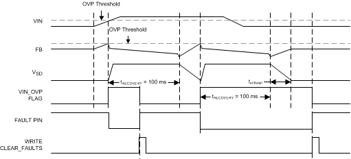 Figure 37. Input OVP Triggering and Recovery
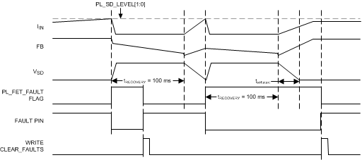 Figure 39. Input OVP Triggering and Recovery
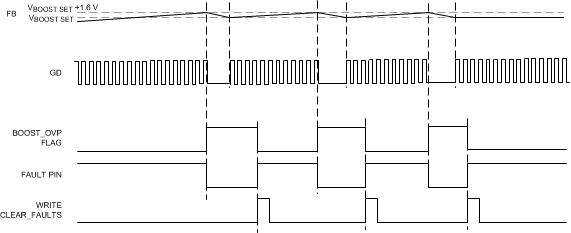 Figure 41. Boost OVP Triggering and Recovery
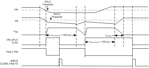 Figure 38. Input UVLO Triggering and Recovery
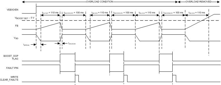 Figure 40. Boost OCP Triggering and Recovery
8.4 Device Functional Modes
8.4.1 Standby Mode
The device is in standby mode when the EN/VDDIO pin is low. Current consumption from the VDD pin in this mode is typically 1 µA.
8.4.2 Active Mode
The EN/VDDIO pin enables the logic and analog blocks. The device goes through the start-up sequence where EEPROM context is loaded to the registers, the power-line FET is enabled during soft start, and boost starts during boost start-time. In this mode I2C and SPI communication are available after soft start, and register settings can be changed.
8.4.3 Fault Recovery State
Fault recovery state is special state which can be caused by faults. In this state power line FET is switched off, boost and LED current sinks are disabled. I2C or SPI interfaces are available in this state — for example, fault flags can be read.
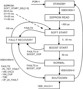 Figure 42. State Diagram
8.4.4 Start-Up and Shutdown Sequences
Depending on EEPROM settings the LP8860-Q1 can be started up or shut down differently. Typical start-up/shutdown sequence is shown in Figure 43.
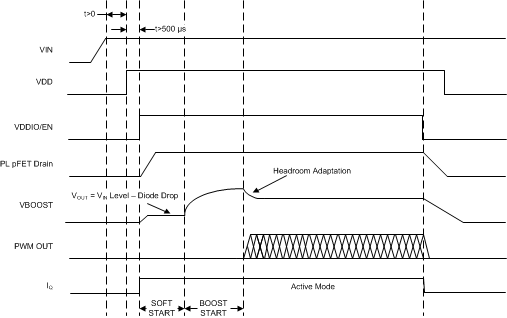 Figure 43. Timing Diagram for the Typical Start-Up and Shutdown
8.5 Programming
8.5.1 EEPROM
EEPROM memory stores various parameters for chip control. The 200-bit EEPROM memory is organized as 25 × 8 bits. The EEPROM structure consists of a register front-end and the non-volatile memory (NVM). Register data can be read and written through the I2C/SPI serial interface. EEPROM must be burned with the new data; otherwise, data disappears after power-on reset or VDDIO/EN cycling. PWM outputs and PLL must be disabled when writing to EEPROM registers or burning EEPROM (<DISP_CL1_BRT[15:0]> = 0, <CL2_BRT[12:0]> = 0, <CL3_BRT[12:0]> = 0, <CL2_BRT[12:0]> = 0, <EN_PLL> = 0). To read and program EEPROM NVM separate commands need to be sent. Erase and program voltages are generated internally; no other voltages other than the normal VDD voltage is required. A complete EEPROM memory map is shown in the Table 23.
The user must make sure that VDD power is on, and the VDDIO/EN pin is kept high, during the whole programming/burn sequence to avoid memory corruption.
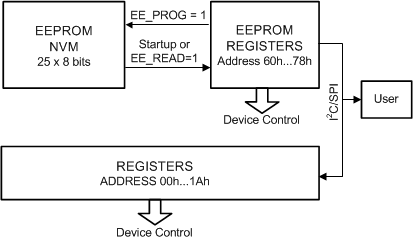 Figure 44. EEPROM and Register Configuration
EEPROM has protection against accidental writes. EEPROM access can be unlocked by writing a pass code to the EEPROM_UNLOCK register. It unlocks the EEPROM Control register EEPROM_CNTRL and all EEPROM registers. Lock is enabled again by writing any other code to the EEPROM_UNLOCK register (for example, 0x00 enables the lock any time).
Table 19. EEPROM Pass Code Protection
| PASS CODE TO EEPROM_UNLOCK REGISTER |
|---|
| 0x08, 0xBA, 0xEF |
EEPROM is used as fixed product-configuration storage, to be set or programmed during production before normal operation. EEPROM can be reprogrammed for evaluation purposes up to 1000 cycles. Data-retention lifetime for factory-programmed content is 10 years, minimum. For more details regarding EEPROM options, see TI Application Note Selecting the Correct LP8860-Q1 EEPROM Version (SNVA757).
8.5.2 Serial Interface
The LP8860-Q1 supports 2 different interface modes:
- SPI interface (4-wire serial)
- I2C-compatible (2-wire serial)
The user can define the interface mode by IF pin as shown in Table 20. The LP8860-Q1 detects interface mode selection during start-up. When the device is in normal mode, the IF signal does not affect the interface selection.
8.5.2.1 SPI Interface
The LP8860-Q1 is compatible with SPI serial-bus specification, and it operates as a slave. The transmission consists of 16-bit write and read cycles. One cycle consists of 7 address bits, 1 read/write (R/W) bit, and 8 data bits. The R/W bit high state defines a write cycle and low defines a read cycle. MISO output is normally in a high-impedance state. When the slave select NSS for LP8680 is active (that is, low), MISO output is pulled low for both read and write operations, except for the period when Data is sent out during a read cycle. The Address and Data are transmitted MSB first. The Slave Select signal NSS must be low during the Cycle transmission. NSS resets the interface when high, and it has to be taken high between successive cycles. Data is clocked in on the rising edge of the SCLK clock signal, while data is clocked out on the falling edge of SCLK.
 Figure 46. SPI Read Cycle
8.5.2.2 I2C Serial Bus Interface
8.5.2.2.1 Interface Bus Overview
The I2C-compatible synchronous serial interface provides access to the programmable functions and registers on the device. This protocol is using a two-wire interface for bi-directional communications between the devices connected to the bus. The two interface lines are the Serial Data Line (SDA), and the Serial Clock Line (SCL). These lines must be connected to a positive supply through a pullup resistor and remain HIGH even when the bus is idle.
Every device on the bus is assigned a unique address and acts as either a Master or a Slave depending on whether it generates or receives the SCL. The LP8860-Q1 is always a slave device.
8.5.2.2.2 Data Transactions
One data bit is transferred during each clock pulse. Data is sampled during the high state of the SCL. Consequently, throughout the clock high period, the data must remain stable. Any changes on the SDA line during the high state of the SCL and in the middle of a transaction, aborts the current transaction. New data must be sent during the low SCL state. This protocol permits a single data line to transfer both command/control information and data using the synchronous serial clock.
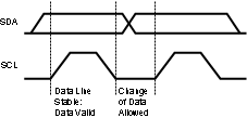 Figure 47. Bit Transfer
Each data transaction is composed of a Start Condition, a number of byte transfers (set by the software) and a Stop Condition to terminate the transaction. Every byte written to the SDA bus must be 8 bits long and is transferred with the most significant bit first. After each byte, an Acknowledge signal must follow. The following sections provide further details of this process.
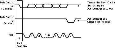 Figure 48. Start and Stop
The Master device on the bus always generates the Start and Stop Conditions (control codes). After a Start Condition is generated, the bus is considered busy and it retains this status until a certain time after a Stop Condition is generated. A high-to-low transition of the data line (SDA) while the clock (SCL) is high indicates a Start Condition. A low-to-high transition of the SDA line while the SCL is high indicates a Stop Condition.
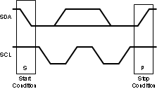 Figure 49. Stop and Start Conditions
In addition to the first Start Condition, a repeated Start Condition can be generated in the middle of a transaction. This allows another device to be accessed, or a register read cycle.
8.5.2.2.3 Acknowledge Cycle
The Acknowledge Cycle consists of two signals: the acknowledge clock pulse the master sends with each byte transferred, and the acknowledge signal sent by the receiving device.
The master generates the acknowledge clock pulse on the ninth clock pulse of the byte transfer. The transmitter releases the SDA line (permits it to go high) to allow the receiver to send the acknowledge signal. The receiver must pull down the SDA line during the acknowledge clock pulse and ensure that SDA remains low during the high period of the clock pulse, thus signaling the correct reception of the last data byte and its readiness to receive the next byte.
8.5.2.2.4 Acknowledge After Every Byte Rule
The master generates an acknowledge clock pulse after each byte transfer. The receiver sends an acknowledge signal after every byte received.
There is one exception to the acknowledge after every byte rule. When the master is the receiver, it must indicate to the transmitter an end of data by not-acknowledging (negative acknowledge”) the last byte clocked out of the slave. This negative acknowledge still includes the acknowledge clock pulse (generated by the master), but the SDA line is not pulled down.
8.5.2.2.5 Addressing Transfer Formats
Each device on the bus has a unique slave address. The LP8860-Q1 operates as a slave device with 7-bit address combined with data direction bit. Default slave address is 2Dh as 7-bit or 5Ah for write and 5Bh for read in 8-bit format.
Before any data is transmitted, the master transmits the address of the slave being addressed. The slave device sends an acknowledge signal on the SDA line, once it recognizes its address. The slave address is the first seven bits after a Start Condition. The direction of the data transfer (R/W) depends on the bit sent after the slave address — the eighth bit. When the slave address is sent, each device in the system compares this slave address with its own. If there is a match, the device considers itself addressed and sends an acknowledge signal. Depending upon the state of the R/W bit (1:read, 0:write), the device acts as a transmitter or a receiver.
 Figure 50. Address and Read/Write Bit
8.5.2.2.6 Control Register Write Cycle
- Master device generates start condition.
- Master device sends slave address (7 bits) and the data direction bit (r/w = “0”).
- Slave device sends acknowledge signal if the slave address is correct.
- Master sends control register address (8 bits).
- Slave sends acknowledge signal.
- Master sends data byte to be written to the address register.
- Slave sends acknowledgement.
- Write cycle ends when the master creates stop condition.
8.5.2.2.7 Control Register Read Cycle
- Master device generates start condition.
- Master device sends slave address (7 bits) and the data direction bit (r/w = “0”).
- Slave device sends acknowledge signal if the slave address is correct.
- Master sends control register address (8 bits).
- Slave sends acknowledge signal if slave address is correct.
- Master generates repeated start condition
- Master sends the slave address (7 bits) and the data direction bit (r/w = “1”)
- Slave sends acknowledgment if the slave address is correct.
- Read cycle ends when master does not generate acknowledge signal after data byte and generates stop condition.
Table 21. Data Read and Write Cycles
| MODE | ACTION(1) |
|---|---|
| Data Read | <Start Condition> |
| <Slave Address><r/w = ‘0’>[Ack] | |
| <Register Addr.>[Ack] | |
| <Repeated Start Condition> | |
| <Slave Address><r/w = ‘1’>[Ack] | |
| [Register Data]<Ack or Nack> | |
| register address possible | |
| <Stop Condition> | |
| Data Write | <Start Condition> |
| <Slave Address><r/w=’0’>[Ack] | |
| <Register Addr.>[Ack] | |
| <Register Data>[Ack] | |
| register address possible | |
| <Stop Condition> |
 Figure 51. Register Write Format
 Figure 52. Register Read Format
8.6 Register Maps
Table 22. Register Map
| ADDR | REGISTER | D7 | D6 | D5 | D4 | D3 | D2 | D1 | D0 |
|---|---|---|---|---|---|---|---|---|---|
| 0x00 | DISP_CL1_BRT | DISP_CL1_BRT[15:8] | |||||||
| 0x01 | DISP_CL1_BRT[7:0] | ||||||||
| 0x02 | DISP_CL1_CURRENT | RESERVED | DISP_CL1_CURRENT[11:8] | ||||||
| 0x03 | DISP_CL1_CURRENT[7:0] | ||||||||
| 0x04 | CL2_BRT | RESERVED | CL2_BRT[12:8] | ||||||
| 0x05 | CL2_BRT[7:0] | ||||||||
| 0x06 | CL2_CURRENT | CL2_CURRENT[7:0] | |||||||
| 0x07 | CL3_BRT | RESERVED | CL3_BRT[12:8] | ||||||
| 0x08 | CL3_BRT[7:0] | ||||||||
| 0x09 | CL3_CURRENT | CL3_CURRENT[7:0] | |||||||
| 0x0A | CL4_BRT | RESERVED | CL4_BRT[12:8] | ||||||
| 0x0B | CL4_BRT[7:0] | ||||||||
| 0x0C | CL4_CURRENT | CL4_CURRENT[7:0] | |||||||
| 0x0D | CONFIGURATION | RESERVED | DRV_LED_CURENT_SCALE[2:0] | EN_ADVANCED_ SLOPE |
PWM_SLOPE[2:0] | ||||
| 0x0E | STATUS | RESERVED | BRT_SLOPE_ DONE |
TEMP_RES_ MISSING |
EXT_TEMP_ FLAG_L |
EXT_TEMP_ FLAG_H |
|||
| 0x0F | FAULT | RESERVED | VIN_OVP | VIN_UVLO | TSD | BOOST_OCP | BOOST_OVP | PL_FET_ FAULT |
CP_2X_ FAULT |
| 0x10 | LED FAULT | RESERVED | OPEN_LED | SHORT_LED | LED_FAULT[4:1] | ||||
| 0x11 | FAULT CLEAR | RESERVED | CLEAR_FAULTS | ||||||
| 0x12 | ID | FULL_LAYER_REVISION | METAL_REVISION | ||||||
| 0x13 | TEMP MSB | RESERVED | TEMP[10:8] | ||||||
| 0x14 | TEMP LSB | TEMP[7:0] | |||||||
| 0x15 | DISP LED CURRENT | RESERVED | LED_CURRENT[11:8] | ||||||
| 0x16 | LED_CURRENT[7:0] | ||||||||
| 0x17 | DISP LED PWM | PWM[15:8] | |||||||
| 0x18 | PWM[7:0] | ||||||||
| 0x19 | EEPROM_CNTRL | EE_READY | RESERVED | EE_PROG | EE_READ | ||||
| 0x1A | EEPROM_UNLOCK | EEPROM_UNLOCK_CODE[7:0] | |||||||
Table 23. EEPROM Register Map(1)
| ADDR | REGISTER | D7 | D6 | D5 | D4 | D3 | D2 | D1 | D0 |
|---|---|---|---|---|---|---|---|---|---|
| 0x60 | EEPROM REG 0 | EXT_TEMP_MINUS[1:0] | DRV_LED_BIAS_CTRL[1:0] | LED_CURRENT_CTRL[11:8] | |||||
| 0x61 | EEPROM REG 1 | LED_CURRENT_CTRL[7:0] | |||||||
| 0x62 | EEPROM REG 2 | RESERVED | EN_STEADY_ DITHER |
PWM_INPUT_HYSTERESIS[1:0] | EN_ADVANCED_SLOPE | PWM_SLOPE[2:0] | |||
| 0x63 | EEPROM REG 3 | EN_DISPAY_LED_ FAULT |
DRV_LED_CURRENT_SCALE[2:0] | LED_STRING_CONF[2:0] | EN-PWM_I | ||||
| 0x64 | EEPROM REG 4 | EN_CL_LED_ FAULT |
DRV_LED_COMP_HYST[1:0] | DRV_LED_FAULT_THR[1:0] | DRV_HEADR[2:0] | ||||
| 0x65 | EEPROM REG 5 | I_SLOPE[2:0] | PWM_RESOLUTION[1:0] | DITHER[2:0] | |||||
| 0x66 | EEPROM REG 6 | RESERVED | GAIN_CTRL[2:0] | DRV_EN_EXT_ LED_CUR_CTR |
DRV_EN_SPLIT_FET | BRT_MODE[1:0] | |||
| 0x67 | EEPROM REG 7 | DRV_OUT2_CORR[3:0] | DRV_OUT1_CORR[3:0] | ||||||
| 0x68 | EEPROM REG 8 | DRV_OUT4_CORR[3:0] | DRV_OUT3_CORR[3:0] | ||||||
| 0x69 | EEPROM REG 9 | EXT_TEMP_GAIN[3:0] | BL_COMP_FILTER_SEL[3:0] | ||||||
| 0x6A | EEPROM REG 10 | EXT_TEMP_I_ DIMMING_EN |
NMOS_PLFET_ EN |
SOFT_START_SEL[1:0] | PL_SD_LEVEL[1:0] | PL_SD_SINK_LEVEL[1:0] | |||
| 0x6B | EEPROM REG 11 | SLOW_PLL_DIV[12:5] | |||||||
| 0x6C | EEPROM REG 12 | EN_SYNC | PWM_SYNC | PWM_ COUNTER_ RESET |
SLOW_PLL_DIV[4:0] | ||||
| 0x6D | EEPROM REG 13 | R_SELL[1:0] | SEL_DIVIDER | EN_PLL | SYNC_PRE_DIVIDER[3:0] | ||||
| 0x6E | EEPROM REG 14 | RESERVED | SYNC_TYPE | PWM_FREQ[3:0] | |||||
| 0x6F | EEPROM REG 15 | MASK_BOOST_ OVP_FSM |
MASK_BOOST_ OCP_FSM |
MASK_OVP_ FSM |
MASK_VIN_ UVLO |
UVLO_LEVEL[1:0] | OVP_LEVEL[1:0] | ||
| 0x70 | EEPROM REG 16 | RESERVED | BOOST_EN_ IRAMP _SU_ DELAY |
BOOST_EXT_ CLK_SEL |
BOOST_IMAX_SEL[2:0] | BOOST_GD_ VOLT |
|||
| 0x71 | EEPROM REG 17 | BOOST_EN_ SPREAD_ SPECTRUM |
BOOST_SEL_IND[1:0] | BOOST_SEL_IRAMP[1:0] | BOOST_FREQ_SEL[2:0] | ||||
| 0x72 | EEPROM REG 18 | BOOST_DRIVER_SIZE[1:0] | EN_ADAP | EN_JUMP | BRIGHTNESS_JUMP_THRES[1:0] | JUMP_STEP_SIZE[1:0] | |||
| 0x73 | EEPROM REG 19 | RESERVED | BOOST_INITIAL_VOLTAGE[5:0] | ||||||
| 0x74 | EEPROM REG 20 | BOOST_SEL_LLC[1:0] | BOOST_SEL_JITTER_FILTER[1:0] | BOOST_SEL_I[1:0] | BOOST_SEL_P[1:0] | ||||
| 0x75 | EEPROM REG 21 | BOOST_OFFTIME_SEL[1:0] | BOOST_BLANKTIME_SEL[1:0] | RESERVED | BOOST_VO_SLOPE_CTRL[2:0] | ||||
| 0x76 | EEPROM REG 22 | VDD_UVLO_LEVEL | RESERVED | CP_2X_CLK[1:0] | CP_2X_EN | SQW_PULSE_ GEN_EN |
|||
| 0x77 | EEPROM REG 23 | EXT_TEMP_LEVEL_HIGH[3:0] | EXT_TEMP_LEVEL_LOW[3:0] | ||||||
| 0x78 | EEPROM REG 24 | INT_TEMP_LIM[1:0] | EXT_TEMP_PERIOD[4:0] | EXT_TEMP_ COMP_EN |
|||||
8.6.1 Register Bit Explanations
8.6.1.1 Display/Cluster1 Brightness Control MSB
Address 0x00
Reset value 0000 0000b
| DISP_CL1_BRT MSB | |||||||
|---|---|---|---|---|---|---|---|
| 7 | 6 | 5 | 4 | 3 | 2 | 1 | 0 |
| DISP_CL1_BRT[15:8] | |||||||
| Name | Bit | Access | Description | ||||
|---|---|---|---|---|---|---|---|
| DISP_CL1_BRT[15:8] | 7:0 | R/W | Backlight brightness control MSB | ||||
8.6.1.2 Display/Cluster1 Brightness Control LSB
Address 0x01
Reset value 0000 0000b
| DISP_CL1_BRT LSB | |||||||
|---|---|---|---|---|---|---|---|
| 7 | 6 | 5 | 4 | 3 | 2 | 1 | 0 |
| DISP_CL1_BRT[7:0] | |||||||
| Name | Bit | Access | Description | ||||
|---|---|---|---|---|---|---|---|
| DISP_CL1_BRT LSB | 7:0 | R/W | Backlight brightness control LSB | ||||
The DISP_CL1_BRT MSB register must be written first. New value is valid after writing DISP_CL1_BRT LSB. If output 1 is used in display mode, the Brightness/Cluster Output 1 Brightness Control register is used for all outputs in display mode (16-bits register). Otherwise it is the Brightness Control register for cluster output 1. For cluster bit control is 13 bit, most significant bit are used.
8.6.1.3 Display/Cluster1 Output Current MSB
Address 0x02
Reset value loaded during start-up from EEPROM REG0
| DISP_CL1_CURRENT MSB | |||||||
|---|---|---|---|---|---|---|---|
| 7 | 6 | 5 | 4 | 3 | 2 | 1 | 0 |
| RESERVED | DISP_CL1_CURRENT[11:8] | ||||||
| Name | Bit | Access | Description | |
|---|---|---|---|---|
| DISP_CL1_CURRENT[11:8] | 3:0 | R/W | Display/Cluster current control MSB | |
8.6.1.4 Display/Cluster1 Output Current LSB
Address 0x03
Reset value loaded during start-up from EEPROM REG1
| DISP_CL1_CURRENT LSB | |||||||
|---|---|---|---|---|---|---|---|
| 7 | 6 | 5 | 4 | 3 | 2 | 1 | 0 |
| DISP_CL1_CURRENT[7:0] | |||||||
| Name | Bit | Access | Description | ||||
|---|---|---|---|---|---|---|---|
| DISP_CL1_CURRENT[7:0] | 7:0 | R/W | Display/Cluster current control LSB | ||||
The DISP_CL1_CURRENT MSB register must be written first. New value is valid after writing DISP_CL1_CURRENT LSB. If one of few outputs is used in display mode, the DISP_CL1_CURRENT register is used for all outputs in display mode (12-bit), otherwise it is Cluster1 Output Current register.
Maximum current is defined by DRV_LED_CURRENT_SCALE[2:0] bits.
8.6.1.5 Cluster2 Brightness Control MSB
Address 0x04
Reset value 0000 0000b
| CL2_BRT MSB | |||||||
|---|---|---|---|---|---|---|---|
| 7 | 6 | 5 | 4 | 3 | 2 | 1 | 0 |
| RESERVED | CL2_BRT[12:8] | ||||||
| Name | Bit | Access | Description | ||||
|---|---|---|---|---|---|---|---|
| CL2_BRT[12:8] | 4:0 | R/W | Cluster output 2 brightness control MSB | ||||
8.6.1.6 Cluster2 Brightness Control LSB
Address 0x05
Reset value 0000 0000b
| CL2_BRT LSB | |||||||
|---|---|---|---|---|---|---|---|
| 7 | 6 | 5 | 4 | 3 | 2 | 1 | 0 |
| CL2_BRT[7:0] | |||||||
| Name | Bit | Access | Description | ||||
|---|---|---|---|---|---|---|---|
| CL2_BRT[7:0] | 7:0 | R/W | Cluster output 2 brightness control LSB | ||||
The CL2_BRT MSB register must be written first. New value is valid after writing CL2_BRT LSB.
8.6.1.7 Cluster2 Output Current
Address 0x06
Reset value 0000 0000b
| CL2_CURRENT | |||||||
|---|---|---|---|---|---|---|---|
| 7 | 6 | 5 | 4 | 3 | 2 | 1 | 0 |
| CL2_CURRENT[7:0] | |||||||
| Name | Bit | Access | Description | ||||
|---|---|---|---|---|---|---|---|
| CL2_CURRENT[7:0] | 7:0 | R/W | Cluster output 2 current control | ||||
Maximum current is defined by DRV_LED_CURRENT_SCALE[2:0] bits.
8.6.1.8 Cluster3 Brightness Control MSB
Address 0x07
Reset value 0000 0000b
| CL3_BRT MSB | |||||||
|---|---|---|---|---|---|---|---|
| 7 | 6 | 5 | 4 | 3 | 2 | 1 | 0 |
| RESERVED | CL3_BRT[12:8] | ||||||
| Name | Bit | Access | Description | ||||
|---|---|---|---|---|---|---|---|
| CL3_BRT[12:8] | 4:0 | R/W | Cluster output 3 brightness control MSB | ||||
8.6.1.9 Cluster3 Brightness Control LSB
Address 0x08
Reset value 0000 0000b
| CL3_BRT LSB | |||||||
|---|---|---|---|---|---|---|---|
| 7 | 6 | 5 | 4 | 3 | 2 | 1 | 0 |
| CL3_BRT[7:0] | |||||||
| Name | Bit | Access | Description | ||||
|---|---|---|---|---|---|---|---|
| CL3_BRT[7:0] | 7:0 | R/W | Cluster output 3 brightness control LSB | ||||
The CL3_BRT MSB register must be written first. New value is valid after writing CL3_BRT LSB.
8.6.1.10 Cluster3 Output Current
Address 0x09
Reset value 0000 0000b
| CL3_CURRENT | |||||||
|---|---|---|---|---|---|---|---|
| 7 | 6 | 5 | 4 | 3 | 2 | 1 | 0 |
| CL3_CURRENT[7:0] | |||||||
| Name | Bit | Access | Description | ||||
|---|---|---|---|---|---|---|---|
| CL3_CURRENT[7:0] | 7:0 | R/W | Cluster output 3 current control | ||||
Maximum current is defined by DRV_LED_CURRENT_SCALE[2:0] bits.
8.6.1.11 Cluster4 Brightness Control MSB
Address 0x0A
Reset value 0000 0000b
| CL4_BRT MSB | |||||||
|---|---|---|---|---|---|---|---|
| 7 | 6 | 5 | 4 | 3 | 2 | 1 | 0 |
| RESERVED | CL4_BRT[12:8] | ||||||
| Name | Bit | Access | Description | ||||
|---|---|---|---|---|---|---|---|
| CL4_BRT[12:8] | 4:0 | R/W | Cluster output 4 brightness control MSB | ||||
8.6.1.12 Cluster4 Brightness Control LSB
Address 0x0B
Reset value 0000 0000b
| CL4_BRT LSB | |||||||
|---|---|---|---|---|---|---|---|
| 7 | 6 | 5 | 4 | 3 | 2 | 1 | 0 |
| CL4_BRT[7:0] | |||||||
| Name | Bit | Access | Description | ||||
|---|---|---|---|---|---|---|---|
| CL4_BRT[7:0] | 7:0 | R/W | Cluster output 4 brightness control LSB | ||||
The CL4_BRT MSB register must be written first. New value is valid after writing CL4_BRT LSB.
8.6.1.13 Cluster4 Output Current
Address 0x0C
Reset value 0000 0000b
| CL4_CURRENT | |||||||
|---|---|---|---|---|---|---|---|
| 7 | 6 | 5 | 4 | 3 | 2 | 1 | 0 |
| CL4_CURRENT[7:0] | |||||||
| Name | Bit | Access | Description | ||||
|---|---|---|---|---|---|---|---|
| CL4_CURRENT[7:0] | 7:0 | R/W | Cluster output 4 current control | ||||
Maximum current is defined by DRV_LED_CURRENT_SCALE[2:0] bits.
8.6.1.14 Configuration
Address 0x0D
Reset value loaded during start-up from EEPROM
| CONFIGURATION | |||||||
|---|---|---|---|---|---|---|---|
| 7 | 6 | 5 | 4 | 3 | 2 | 1 | 0 |
| RESERVED | DRV_LED_CURRENT_SCALE[2:0] | EN_ADVANCED _SLOPE |
PWM_SLOPE[2:0] | ||||
| Name | Bit | Access | Description | ||||
|---|---|---|---|---|---|---|---|
| DRV_LED_CURRENT_SCALE[2:0] | 6:4 | R/W | Scales the maximum LED current when EN_EXT_LED_CUR_CTRL = 0 Effective for display and cluster mode. 000 = 25 mA 001 = 30 mA 010 = 50 mA 011 = 60 mA 100 = 80 mA 101 = 100 mA 110 = 120 mA 111 = 150 mA |
||||
| EN_ADVANCED_SLOPE | 3 | R/W | Enable for advanced slope (smooth brightness change) 0 = Linear slope used only 1 = Advanced slope used |
||||
| PWM_SLOPE[2:0] | 2:0 | R/W | Linear brightness sloping time (typical) 000 = 0 ms 001 = 1 ms 010 = 2 ms 011 = 52 ms 100 = 105 ms 101 = 210 ms 110 = 315 ms 111 = 511 ms |
||||
8.6.1.15 Status
Address 0x0E
Reset value 0000 0000b
| STATUS | |||||||
|---|---|---|---|---|---|---|---|
| 7 | 6 | 5 | 4 | 3 | 2 | 1 | 0 |
| RESERVED | BRT_SLOPE_DONE | TEMP_RES_MISSING | EXT_TEMP_FLAG_L | EXT_TEMP_FLAG_H | |||
| Name | Bit | Access | Description | ||||
|---|---|---|---|---|---|---|---|
| BRT_SLOPE_DONE | 3 | R | Status bit for the brightness sloping 0 = Sloping ongoing 1 = Sloping done |
||||
| TEMP_RES_MISSING | 2 | R | NTC sensor missing flag 0 = sensor OK 1 = NTC sensor missing |
||||
| EXT_TEMP_FLAG_L | 1 | R | External temperature sensor low limit exceeded flag 0 = limit not detected 1 = low temperature limit detected |
||||
| EXT_TEMP_FLAG_H | 0 | R | External temperature sensor high limit exceeded flaf 0 = limit not detected 1 = high temperature limit detected |
||||
8.6.1.16 Fault
Address 0x0F
Reset value 0000 0000b
| STATUS | |||||||
|---|---|---|---|---|---|---|---|
| 7 | 6 | 5 | 4 | 3 | 2 | 1 | 0 |
| RESERVED | VIN_OVP | VIN_UVLO | TSD | BOOST_OCP | BOOST_OVP | PL_FET_FAULT | CP_2X_FAULT |
| Name | Bit | Access | Description | ||||
|---|---|---|---|---|---|---|---|
| VIN_OVP | 6 | R | VIN overvoltage protection flag 0 = No fault 1 = Fault detected |
||||
| VIN_UVLO | 5 | R | VIN undervoltage lockout flag 0 = No fault 1 = Fault detected |
||||
| TSD | 4 | R | Thermal shutdown 0 = No flag 1 = Fault detected |
||||
| BOOST_OCP | 3 | R | Boost overcurrent protection flag 0 = No flag 1 = Fault detected |
||||
| BOOST_OVP | 2 | R | Boost output overvoltage protection flag 0 = No flag 1 = Fault detected |
||||
| PL_FET_FAULT | 1 | R | VIN overcurrent protection flag 0 = No fault 1 = Fault detected |
||||
| CP_2X_FAULT | 0 | R | Charge pump output voltage too low 0 = No fault 1 = Fault detected |
||||
8.6.1.17 LED Fault
Address 0x10
Reset value 0000 0000b
| LED FAULT | |||||||
|---|---|---|---|---|---|---|---|
| 7 | 6 | 5 | 4 | 3 | 2 | 1 | 0 |
| RESERVED | OPEN_LED | SHORT_LED | LED_FAULT[4:1] | ||||
| Name | Bit | Access | Description | ||||
|---|---|---|---|---|---|---|---|
| OPEN_LED | 5 | R | Open LED fault. 0 = No fault 1 = Fault detected |
||||
| SHORT_LED | 4 | R | Short LED fault. 0 = No fault 1 = Fault detected |
||||
| LED_FAULT[4:1] | 3:0 | R | Defines which string has either open or short fault. 0001 = LED OUT1 0010 = LED OUT2 0100 = LED OUT3 1000 = LED OUT4 |
||||
8.6.1.18 Fault Clear
Address 0x11
Reset value 0000 0000b
| FAULT CLEAR | |||||||
|---|---|---|---|---|---|---|---|
| 7 | 6 | 5 | 4 | 3 | 2 | 1 | 0 |
| RESERVED | CLEAR_FAULTS | ||||||
| Name | Bit | Access | Description | ||||
|---|---|---|---|---|---|---|---|
| CLEAR_FAULTS | 0 | W | Write only bit, writing CLEAR_FAULTS high clears faults. | ||||
8.6.1.19 Identification
Address 0x12
| ID | |||||||
|---|---|---|---|---|---|---|---|
| 7 | 6 | 5 | 4 | 3 | 2 | 1 | 0 |
| FULL_LAYER_REVISION[3:0] | METAL REVISIONS[3:0] | ||||||
| Name | Bit | Access | Description | ||||
|---|---|---|---|---|---|---|---|
| FULL_LAYER_REVISION | 7:4 | R | Manufacturer ID code – full layer revision | ||||
| METAL REVISIONS | 3:0 | R | Manufacturer ID code – metal mask revision | ||||
8.6.1.20 Temp MSB
Address 0x13
| TEMP MSB | |||||||
|---|---|---|---|---|---|---|---|
| 7 | 6 | 5 | 4 | 3 | 2 | 1 | 0 |
| RESERVED | TEMP[10:8] | ||||||
| Name | Bit | Access | Description | ||||
|---|---|---|---|---|---|---|---|
| TEMP[10:8] | 2:0 | R | Device internal temperature sensor reading, first 3 MSB. MSB must be read before LSB, because reading of MSB register latches the data. | ||||
8.6.1.21 Temp LSB
Address 0x14
| TEMP LSB | |||||||
|---|---|---|---|---|---|---|---|
| 7 | 6 | 5 | 4 | 3 | 2 | 1 | 0 |
| TEMP[7:0] | |||||||
| Name | Bit | Access | Description | ||||
|---|---|---|---|---|---|---|---|
| TEMP[7:0] | 7:0 | R | Device internal temperature sensor reading, last 8 LSB. MSB must be read before LSB, because reading of MSB register latches the data. | ||||
8.6.1.22 Display LED Current MSB
Address 0x15
| DISP LED CURRENT MSB | |||||||
|---|---|---|---|---|---|---|---|
| 7 | 6 | 5 | 4 | 3 | 2 | 1 | 0 |
| RESERVED | LED_CURRENT[11:8] | ||||||
| Name | Bit | Access | Description | ||||
|---|---|---|---|---|---|---|---|
| LED_CURRENT[11:8] | 3:0 | R | Display LED current value reading, first 3 MSB. DISP LED CURRENT MSB must be read before DISP LED CURRENT LSB, DISP LED PWM MSB, and DISP LED PWM LSB because reading of the MSB register latches the data for current and PWM. | ||||
8.6.1.23 Display LED Current LSB
Address 0x16
| DISP LED CURRENT LSB | |||||||
|---|---|---|---|---|---|---|---|
| 7 | 6 | 5 | 4 | 3 | 2 | 1 | 0 |
| LED_CURRENT[7:0] | |||||||
| Name | Bit | Access | Description | ||||
|---|---|---|---|---|---|---|---|
| LED_CURRENT[7:0] | 7:0 | R | Display LED current value reading, last 8 LSB. Note: DISP LED CURRENT MSB latches the data for current and PWM. |
||||
8.6.1.24 Display LED PWM MSB
Address 0x17
Reset value 0000 0000b
| DISP LED PWM MSB | |||||||
|---|---|---|---|---|---|---|---|
| 7 | 6 | 5 | 4 | 3 | 2 | 1 | 0 |
| PWM[15:8] | |||||||
| Name | Bit | Access | Description | ||||
|---|---|---|---|---|---|---|---|
| PWM[7:0] | 7:0 | R | Display LED current value reading, first 8 MSB. Note: DISP LED CURRENT MSB latches the data for current and PWM. |
||||
8.6.1.25 Display LED PWM LSB
Address 0x18
Reset value 0000 0000b
| DISP LED PWM LSB | |||||||
|---|---|---|---|---|---|---|---|
| 7 | 6 | 5 | 4 | 3 | 2 | 1 | 0 |
| PWM[7:0] | |||||||
| Name | Bit | Access | Description | ||||
|---|---|---|---|---|---|---|---|
| PWM[7:0] | 7:0 | R | Display LED PWM reading, last 8 LSB. Note: DISP LED CURRENT MSB latches the data for current and PWM. |
||||
8.6.1.26 EEPROM Control
Address 0x19
Reset value 1000 0000b
| EEPROM CTRL | |||||||
|---|---|---|---|---|---|---|---|
| 7 | 6 | 5 | 4 | 3 | 2 | 1 | 0 |
| EE_READY | RESERVED | EE_PROG | EE_READ | ||||
| Name | Bit | Access | Description |
|---|---|---|---|
| EE_READY | 7 | R | EEPROM ready 0 = EEPROM programming or read in progress 1 = EEPROM ready, not busy |
| EE_PROG | 1 | R/W | EEPROM programming 0 = Normal operation 1 = Start the EEPROM programming sequence. Programs data currently in the EEPROM registers to non-volatile memory (NVM). |
| EE_READ | 0 | R/W | EEPROM read 0 = Normal operation 1 = Reads the data from NVM to the EEPROM registers. Can be used to restore default values if EEPROM registers are changed during testing. |
Programming sequence (program data permanently from registers to NVM):
- Turn on the chip by setting VDDIO/EN pin high.
- Unlock EEPROM by writing the unlock codes to register 0x1A.
- Write 0x08 to address 0x1A
- Write 0xBA to address 0x1A
- Write 0xEF to address 0x1A
- Write data to EEPROM registers (address 0x60…0x78).
- Write EE_PROG to high in address 0x19. (0x02 to address 0x19).
- Wait 200 ms.
- Write EE_PROG to low in address 0x19. (0x00 to address 0x19).
Read sequence (load data from NVM to registers):
- Turn on the chip by writing setting VDDIO/EN pin high.
- Unlock EEPROM by writing the unlock codes to register 0x1A.
- Write 0x08 to address 0x1A
- Write 0xBA to address 0x1A
- Write 0xEF to address 0x1A
- Write EE_READ to high in address 0x19. (0x01 to address 0x19).
- Wait 1 ms.
- Write EE_READ to low in address 0x19. (0x00 to address 0x19).
NOTE
EEPROM bits are intended to be set/programmed before normal operation only once during silicon production, but can be reprogrammed for evaluation purposes up to 1000 cycles.
8.6.1.27 EEPROM Unlock Code
Address 0x1A
Reset value 0000 0000b
| EEPROM UNLOCK | |||||||
|---|---|---|---|---|---|---|---|
| 7 | 6 | 5 | 4 | 3 | 2 | 1 | 0 |
| EEPROM UNLOCK_CODE[7:0] | |||||||
| Name | Bit | Access | Description |
|---|---|---|---|
| EEPROM_UNLOCK_CODE[7:0] | 7:0 | W | Unlock EEPROM control register (0x19) and EEPROM registers. Writing 0x08, 0xBA, 0xEF sequence unlocks EEPROM registers. Lock is enabled again by writing any other code to the register. |
8.6.2 EEPROM Bit Explanations
8.6.2.1 EEPROM Register 0
| EEPROM REGISTER 0 | |||||||
|---|---|---|---|---|---|---|---|
| 7 | 6 | 5 | 4 | 3 | 2 | 1 | 0 |
| EXT_TEMP_MINUS[1:0] | DRV_LED_BIAS_CTRL[1:0] | LED_CURRENT_CTRL[11:8] | |||||
| Name | Bit | Access | Description | ||||
|---|---|---|---|---|---|---|---|
| EXT_TEMP_MINUS[1:0] | 7:6 | R/W | External temperature sensor current dimming knee point, see LED Current Dimming With Internal Temperature Sensor for details. 00 = 1 μA 01 = 5 μA 10 = 9 μA 11 = 13 μA |
||||
| DRV_LED_BIAS_CTRL[1:0] | 5:4 | R/W | Controls the LED current sink bias current. Effects LED current sink rise time and current consumption. 150-mA LED current is suggested. 00 = slowest LED current sink setting and low Iq (typical 800-ns rise time / 200 μA per sink) 01 = slow (typical 400-ns rise time / 400 μA per sink) 10 = fast (typical 200-ns rise time / 800 μA per sink) 11 = fastest LED current sink and higher current consumption (typical100-ns rise time / 1.6 mA per sink) |
||||
| LED_CURRENT_CTRL[11:8] | 3:0 | R/W | MSB bits for 12-bit LED current control. Step size is 150 mA / 4095 = 36.63 µA (typical) when max current is set to 150 mA. Max current can be scaled with RISET resistor or with DRV_LED_CURRENT_SCALE EEPROM bits. 000h = 0 mA 001h = 0.037 mA 002h = 0.073 mA 003h = 0.110 mA … FFEh = 149.963 mA FFFh = 150.000 mA |
||||
8.6.2.2 EEPROM Register 1
Address 0x61
| EEPROM REGISTER 1 | |||||||
|---|---|---|---|---|---|---|---|
| 7 | 6 | 5 | 4 | 3 | 2 | 1 | 0 |
| LED_CURRENT_CTRL[7:0] | |||||||
| Name | Bit | Access | Description | ||||
|---|---|---|---|---|---|---|---|
| LED_CURRENT_CTRL[7:0] | 7:0 | R/W | LSB bits for 12-bit LED current control. Step size is 150 mA / 4095 = 36.63 µA when max current is set to 150 mA. Max current can be scaled with RISET resistor or with DRV_LED_CURRENT_SCALE EEPROM bits. 000h = 0 mA 001h = 0.037 mA 002h = 0.073 mA 003h = 0.110 mA … FFEh = 149.963 mA FFFh = 150.000 mA |
||||
8.6.2.3 EEPROM Register 2
Address 0x62
| EEPROM REGISTER 2 | |||||||
|---|---|---|---|---|---|---|---|
| 7 | 6 | 5 | 4 | 3 | 2 | 1 | 0 |
| RESERVED | EN_STEADY_DITHER | PWM_INPUT_HYSTERESIS[1:0] | EN_ADVANCED_SLOPE | PWM_SLOPE[2:0] | |||
8.6.2.4 EEPROM Register 3
Address 0x63
| EEPROM REGISTER 3 | |||||||
|---|---|---|---|---|---|---|---|
| 7 | 6 | 5 | 4 | 3 | 2 | 1 | 0 |
| EN_DISPLAY_LED_FAULT | DRV_LED_CURRENT_SCALE[2:0] | LED_STRING_CONF[2:0] | EN_PWM_I | ||||
| Name | Bit | Access | Description | ||||
|---|---|---|---|---|---|---|---|
| EN_DISPLAY_LED_FAULT | 7 | R/W | 0 = LED open/short faults disabled 1 = LED open/short faults enabled |
||||
| DRV_LED_CURRENT_SCALE[2:0] | 6:4 | R/W | Scales the maximum LED current when EN_EXT_LED_CUR_CTRL = 0 Effective for both modes – display and cluster. 000 = 25 mA 001 = 30 mA 010 = 50 mA 011 = 60 mA 100 = 80 mA 101 = 100 mA 110 = 120 mA 111 = 150 mA |
||||
| LED_STRING_CONF[2:0] | 3:1 | R/W | LED current sink configuration 000 = 4 separate LED strings with 90° phase shift 001 = 3 separate LED strings with 120° phase shift (String 4 in cluster mode or not used) 010 = 2 separate LED strings with 180° phase shift (Strings 3 and 4 in cluster mode or not used) 011 = 1 LED string. (Strings 2,3 and 4 in cluster mode or not used) 100 = 2 LED strings (1+2, 3+4) with 180° phase shift. Tied strings with same phase. 101 = 1 LED string (1+2+3+4). Tied strings with same phase 110 = 1 LED string (1+2). 1st and 2nd strings tied with same phase, strings 3 and 4 are in cluster mode or not used 111 = All strings are used in cluster mode |
||||
| EN_PWM_I | 0 | R/W | Enable Hybrid PWM and Current dimming mode 0 = Disabled, dimming only with PWM 1 = Enabled |
||||
8.6.2.5 EEPROM Register 4
Address 0x64
| EEPROM REGISTER 4 | |||||||
|---|---|---|---|---|---|---|---|
| 7 | 6 | 5 | 4 | 3 | 2 | 1 | 0 |
| EN_CL_LED_FAULT | DRV_LED_COMP_HYST[1:0] | DRV_LED_FAULT_THR[1:0] | DRV_HEADER[2:0] | ||||
8.6.2.6 EEPROM Register 5
Address 0x65
| EEPROM REGISTER 5 | |||||||
|---|---|---|---|---|---|---|---|
| 7 | 6 | 5 | 4 | 3 | 2 | 1 | 0 |
| I_SLOPE[2:0] | PWM_RESOLUTION[1:0] | DITHER[2:0] | |||||
8.6.2.7 EEPROM Register 6
Address 0x66
| EEPROM Register 6 | |||||||
|---|---|---|---|---|---|---|---|
| 7 | 6 | 5 | 4 | 3 | 2 | 1 | 0 |
| RESERVED | GAIN_CTRL[2:0] | EN_EXT_LED_CUR_CTRL | DRV_EN_SPLIT_FET | BRT_MODE[1:0] | |||
| Name | Bit | Access | Description |
|---|---|---|---|
| GAIN_CTRL[2:0] | 6:4 | R/W | Switch point from PWM to current control for Hybrid PWM and Current dimming mode 000 = 50.0% 001 = 40.6% 010 = 31.3% 011 = 25.0% 100 = 21.9% 101 = 18.8% 110 = 15.6% 111 = 12.5% |
| EN_EXT_LED_CUR_CTRL | 3 | R/W | Enable LED current set resistor 0 = Resistor is disabled and current is scaled with SCALE[2:0] EEPROM register bits 1 = Enable LED current set resistor. LED current is scaled by the RISET resistor |
| DRV_EN_SPLIT_FET | 2 | R/W | LED current sink FET control 0 = big size FET is driving LED current 1 = enable use of smaller FET for driving low LED output currents. Smaller FET is selected automatically when current setting is below 1/16 of the scale. Automatic scaling improves accuracy for output currents below 1/16 of the full current scale. |
| BRT_MODE[1:0] | 1:0 | R/W | Brightness control mode 00 = PWM input pin duty cycle control 01 = PWM input duty x Brightness register 10 = Brightness register 11 = Direct PWM control from PWM input pin |
8.6.2.8 EEPROM Register 7
Address 0x67
| EEPROM Register 7 | |||||||
|---|---|---|---|---|---|---|---|
| 7 | 6 | 5 | 4 | 3 | 2 | 1 | 0 |
| DRV_OUT2_CORR[3:0] | DRV_OUT1_CORR[3:0] | ||||||
| Name | Bit | Access | Description |
|---|---|---|---|
| DRV_OUT2_CORR[3:0] | 7:4 | R/W | Current correction for OUT2 LED current sink 0000 = 6.5% 0001 = 5.6% 0010 = 4.7% 0011 = 3.7% 0100 = 2.8% 0101 = 1.9% 0110 = 0.9% 0111 = 0.0% 1000 = –0.9% 1001 = –1.9% 1010 = –2.8% 1011 = –3.7% 1100 = –4.7% 1101 = –5.6% 1110 = –6.5% 1111 = –7.4% |
| DRV_OUT1_CORR[3:0] | 3:0 | R/W | Current correction for OUT1 LED current sink 0000 = 6.5% 0001 = 5.6% 0010 = 4.7% 0011 = 3.7% 0100 = 2.8% 0101 = 1.9% 0110 = 0.9% 0111 = 0.0% 1000 = –0.9% 1001 = –1.9% 1010 = –2.8% 1011 = –3.7% 1100 = –4.7% 1101 = –5.6% 1110 = –6.5% 1111 = –7.4% |
8.6.2.9 EEPROM Register 8
Address 0x68
| EEPROM Register 8 | |||||||
|---|---|---|---|---|---|---|---|
| 7 | 6 | 5 | 4 | 3 | 2 | 1 | 0 |
| DRV_OUT4_CORR[3:0] | DRV_OUT3_CORR[3:0] | ||||||
| Name | Bit | Access | Description |
|---|---|---|---|
| DRV_OUT4_CORR[3:0] | 7:4 | R/W | Current correction for OUT4 LED current sink 0000 = 6.5% 0001 = 5.6% 0010 = 4.7% 0011 = 3.7% 0100 = 2.8% 0101 = 1.9% 0110 = 0.9% 0111 = 0.0% 1000 = –0.9% 1001 = –1.9% 1010 = –2.8% 1011 = –3.7% 1100 = –4.7% 1101 = –5.6% 1110 = –6.5% 1111 = –7.4% |
| DRV_OUT3_CORR[3:0] | 3:0 | R/W | Current correction for OUT3 LED current sink 0000 = 6.5% 0001 = 5.6% 0010 = 4.7% 0011 = 3.7% 0100 = 2.8% 0101 = 1.9% 0110 = 0.9% 0111 = 0.0% 1000 = –0.9% 1001 = –1.9% 1010 = –2.8% 1011 = –3.7% 1100 = –4.7% 1101 = –5.6% 1110 = –6.5% 1111 = –7.4% |
8.6.2.10 EEPROM Register 9
Address 0x69
| EEPROM Register 8 | |||||||
|---|---|---|---|---|---|---|---|
| 7 | 6 | 5 | 4 | 3 | 2 | 1 | 0 |
| EXT_TEMP_GAIN[3:0] | BL_COMP_FILTER_SEL[3:0] | ||||||
| Name | Bit | Access | Description |
|---|---|---|---|
| EXT_TEMP_GAIN[3:0] | 7:4 | R/W | External temperature sensor current dimming gain control, see LED Current Dimming With Internal Temperature Sensor for details. |
| BL_COMP_FILTER_SEL[3:0] | 3:0 | R/W | Filter selects how many PWM generator clock cycles high/mid comparator is filtered before it is used to detect shorted LEDs and boost voltage down scaling. 0000 = 5 0001 = 10 0010 = 20 0011 = 40 0100 = 60 0101 = 80 0110 = 100 0111 = 140 1000 = 180 1001 = 220 1010 = 260 1011 = 300 1100 = 340 1101 = 380 1110 = 420 1111 = 460 |
8.6.2.11 EEPROM Register 10
Address 0x6A
| EEPROM Register 9 | |||||||
|---|---|---|---|---|---|---|---|
| 7 | 6 | 5 | 4 | 3 | 2 | 1 | 0 |
| EXT_TEMP_I_DIMMING_EN | NMOS_PLFET_EN | SOFT_START_SEL[1:0] | PL_SD_LEVEL[1:0] | PL_SD_SINK_LEVEL[1:0] | |||
8.6.2.12 EEPROM Register 11
Address 0x6B
| EEPROM Register 11 | |||||||
|---|---|---|---|---|---|---|---|
| 7 | 6 | 5 | 4 | 3 | 2 | 1 | 0 |
| SLOW_PLL_DIV[12:5] | |||||||
| Name | Bit | Access | Description |
|---|---|---|---|
| SLOW_PLL_DIV[12:5] | 7:0 | R/W | Divider for VSYNC operation. 8 MSB bits |
8.6.2.13 EEPROM Register 12
Address 0x6C
| EEPROM Register 12 | |||||||
|---|---|---|---|---|---|---|---|
| 7 | 6 | 5 | 4 | 3 | 2 | 1 | 0 |
| EN_SYNC | PWM_SYNC | PWM_COUNTER_RESET | SLOW_PLL_DIV[4:0] | ||||
| Name | Bit | Access | Description |
|---|---|---|---|
| EN_SYNC | 7 | R/W | VSYNC input enable 0 = VSYNC input disabled 1 = VSYNC input enabled |
| PWM_SYNC | 6 | R/W | Enable PWM generation synchronization to VSYNC signal 0 = Disabled 1 = Enabled. PWM output used for phase detector input after dividing with SLOW_PLL_DIV divider |
| PWM_COUNTER_RESET | 5 | R/W | Enable PWM generator resetting on VSYNC signal rising edge 0 = Disabled 1 = Enabled |
| SLOW_PLL_DIV[4:0] | 4:0 | R/W | Divider for VSYNC operation. 5 LSB bits |
8.6.2.14 EEPROM Register 13
Address 0x6D
| EEPROM Register 13 | |||||||
|---|---|---|---|---|---|---|---|
| 7 | 6 | 5 | 4 | 3 | 2 | 1 | 0 |
| R_SEL[1:0] | SEL_DIVIDER | EN_PLL | SYNC_PRE_DIVIDER[3:0] | ||||
| Name | Bit | Access | Description |
|---|---|---|---|
| R_SEL[1:0] | 7:6 | R/W | Coefficient for the slow PLL divider 00 = 16 01 = 32 10 = 64 11 = 128 |
| SEL_DIVIDER | 5 | R/W | PLL divider selection 0 = Slow PLL divider with external compensation (when using VSYNC) 1 = Fast PLL divider with internal compensation (when using 5-MHz internal clock) |
| EN_PLL | 4 | R/W | PLL enable 0 = PLL disabled and internal 5-MHz oscillator used for PWM generation 1 = PLL is used for generating the PWM generation clock from the internal oscillator or VSYNC signal |
| SYNC_PRE_DIVIDER[3:0] | 3:0 | R/W | VSYNC signal pre-divider from 1 to 16. Used when VSYNC frequency is higher than PWM output frequency. |
8.6.2.15 EEPROM Register 14
Address 0x6E
| EEPROM Register 14 | |||||||
|---|---|---|---|---|---|---|---|
| 7 | 6 | 5 | 4 | 3 | 2 | 1 | 0 |
| RESERVED | SYNC_TYPE | PWM_FREQ[3:0] | |||||
| Name | Bit | Access | Description |
|---|---|---|---|
| SYNC_TYPE | 4 | R/W | Type of the VSYNC input. Affects the PLL functionality. 0 = HSYNC (50 to 150 kHz) 1 = VSYNC (50 to 150 Hz) |
| PWM_FREQ[3:0] | 3:0 | R/W | PWM output frequency setting when internal oscillator is used. See Brightness Control (Display Mode) |
8.6.2.16 EEPROM Register 15
Address 0x6F
| EEPROM Register 13 | |||||||
|---|---|---|---|---|---|---|---|
| 7 | 6 | 5 | 4 | 3 | 2 | 1 | 0 |
| MASK_BOOST_OVP_ STATUS |
MASK_BOOST_OCP _FSM |
MASK_OVP_FSM | MASK_VIN_UVLO | UVLO_LEVEL[1:0] | OVP_LEVEL[1:0] | ||
| Name | Bit | Access | Description |
|---|---|---|---|
| MASK_BOOST_OVP_STATUS | 7 | R/W | Boost overvoltage protection enable 0 = Enabled 1 = Fault bit and FAULT pin disabled. |
| MASK_BOOST_OCP_FSM | 6 | R/W | Boost overcurrent protection fault recovery state enable 0 = Enabled 1 = Entering fault recovery state disabled. Fault bit and FAULT pin operate normally. |
| MASK_OVP_FSM | 5 | R/W | VIN overvoltage fault recovery state enable 0 = Enabled 1 = Entering fault recovery state disabled. Fault bit and FAULT pin operate normally. |
| MASK_VIN_UVLO | 4 | R/W | VIN undervoltage lockout fault recovery state enable 0 = Enabled 1 = Entering fault recovery state disabled. Fault bit and FAULT pin operate normally. |
| UVLO_LEVEL[1:0] | 3:2 | R/W | VIN Undervoltage protection thresholds (UVLO) 00 = disabled 01 = 3 V 10 = 5 V 11 = 8 V |
| OVP_LEVEL[1:0] | 1:0 | R/W | VIN Overvoltage protection thresholds (OVP) 00 = disabled 01 = 7 V 10 = 11 V 11 = 22.5 V |
8.6.2.17 EEPROM Register 16
Address 0x70
| EEPROM Register 16 | |||||||
|---|---|---|---|---|---|---|---|
| 7 | 6 | 5 | 4 | 3 | 2 | 1 | 0 |
| RESERVED | BOOST_EN_IRAMP_DELAY | BOOST_EXT_CLK_SEL | BOOST_IMAX_SEL[2:0] | BOOST_GD_VOLT | |||
| Name | Bit | Access | Description |
|---|---|---|---|
| BOOST_EN_IRAMP_DELAY | 5 | R/W | Boost current ramp delay enable (for adjusting conversion ratio/stability, 35% of period) 1 = Delay enabled 0 = Delay disabled |
| BOOST_EXT_CLK_SEL | 4 | R/W | Boost clock selection 0 = Internal clock 1 = External clock (SYNC pin) If external clock selected and sync disappears for 1.5…2 periods, boost automatically switches to using internal oscillator with frequency defined by BOOST_FREQ_SEL[2:0] |
| BOOST_IMAX_SEL[2:0] | 3:1 | R/W | Maximum current limit for boost SW mode. Values below based on 25-mΩ sense resistor value. 000 = 2 A 001 = 3 A 010 = 4 A 011 = 5 A 100 = 6 A 101 = 7 A 110 = 8 A 111 = 9 A |
| BOOST_GD_VOLT | 0 | R/W | Boost gate driver voltage selection 1 = Charge pump output (VGATE DRIVER > 6 V) 0 = VDD |
8.6.2.18 EEPROM Register 17
Address 0x71
| EEPROM Register 17 | |||||||
|---|---|---|---|---|---|---|---|
| 7 | 6 | 5 | 4 | 3 | 2 | 1 | 0 |
| BOOST_EN_SPREAD_ SPECTRUM |
BOOST_SEL_IND[1:0] | BOOST_SEL_IRAMP[1:0] | BOOST_FREQ_SEL[2:0] | ||||
| Name | Bit | Access | Description | ||||
|---|---|---|---|---|---|---|---|
| BOOST_EN_SPREAD_ SPECTRUM |
7 | R/W | Boost spread spectrum (±3% from central frequency, 1.875 kHz modulation frequency) enable 0 = Spread spectrum disabled 1 = Spread spectrum enabled |
||||
| BOOST_SEL_IND[1:0] | 6:5 | R/W | See BOOST_SEL_IRAMP for selecting BOOST_SEL_IND setting | ||||
| BOOST_SEL_IRAMP[1:0] | 4:3 | R/W | Boost artificial current ramp peak value, A/s. Select value higher than IRAMP_GAIN: IRAMP_GAIN =1.2 x 0.5 x (VOUTmax - VINmin)/(0.7 x L x 60000), where VIN, VOUT are boost input and output voltage, L - inductance, H. 25-mΩ RSENSE is suggested. |
||||
| BOOST_SEL_IND[1:0] | |||||||
| BOOST_SEL_IRAMP [1:0] |
00 | 01 | 10 | 11 | |||
| 00 | 130 | 65 | 34 | 29 | |||
| 01 | 88 | 43 | 23 | 20 | |||
| 10 | 56 | 28 | 15 | 13 | |||
| 11 | 37 | 18 | 10 | 8.5 | |||
| BOOST_FREQ_SEL[2:0] | 2:0 | R/W | BOOST_EXT_CLK_SEL=0 Boost output frequency selection (internal oscillator) 000= 100 kHz 001 = 200 kHz 010 = 303 kHz 011 = 400 kHz 100 = 629 kHz 101 = 800 kHz 110 = 1100 kHz 111 = 2200 kHz BOOST_EXT_CLK_SEL=1 Boost output frequency selection (for external sync mode if external sync disappears) 000= 100 kHz 001 = 200 kHz 010 = 303 kHz 011 = 400 kHz 100 = 625 kHz 101 = 833 kHz 110 = 1111 kHz 111 = 2500 kHz |
||||
8.6.2.19 EEPROM Register 18
Address 0x72
| EEPROM Register 16 | |||||||
|---|---|---|---|---|---|---|---|
| 7 | 6 | 5 | 4 | 3 | 2 | 1 | 0 |
| BOOST_DRIVER_SIZE[1:0] | EN_ADAP | EN_JUMP | BRIGHTNESS_JUMP_THRES[1:0] | JUMP_STEP_SIZE[1:0] | |||
| Name | Bit | Access | Description |
|---|---|---|---|
| BOOST_DRIVER_SIZE[1:0] | 7:6 | R/W | Boost gate driver scaling. Affects gate driver peak current and SW node voltage rise/fall times 00 = 0.4/0.45 A (typical) peak sink/source current 01 = 0.75/0.87 A (typical) peak sink/source current 10 = 1.2/1.3 A (typical) peak sink/source current 11 = 1.5/1.7 A (typical) peak sink/source current |
| EN_ADAP | 5 | R/W | Enable boost converter adaptive mode 0 = adaptive mode disabled, boost converter output voltage is set with BOOST_INITIAL_VOLTAGE EEPROM register bits. 1 = adaptive mode enabled. Boost converter start-up voltage is set with BOOST_INITIAL_VOLTAGE EEPROM register bits. Further boost voltage is adapted to the highest LED string VF. If all LED outputs are in cluster mode, adaptive mode is disabled automatically. |
| EN_JUMP | 4 | R/W | Enable large boost voltage jump command for the fast brightness increase. 0 = Normal steps used for boost voltage control 1 = Jump command allowed in boost voltage control |
| BRIGHTNESS_JUMP_THRES[1:0] | 3:2 | R/W | Defines the magnitude of the input brightness change after which jump command is given. 00 = Jump command after 10% brightness change 01 = Jump command after 30% brightness change 10 = Jump command after 50% brightness change 11 = Jump command after 70% brightness change |
| JUMP_STEP_SIZE[1:0] | 1:0 | R/W | Boost control step size that jump command increases backlight boost output voltage 00: 8 steps (1.0 V typ) 01: 16 steps (2.0 V typ) 10: 32 steps (4.0 V typ) 11: 64 steps (8.0 V typ) |
8.6.2.20 EEPROM Register 19
Address 0x73
| EEPROM Register 19 | |||||||
|---|---|---|---|---|---|---|---|
| 7 | 6 | 5 | 4 | 3 | 2 | 1 | 0 |
| RESERVED | BOOST_INITIAL_VOLTAGE[5:0] | ||||||
| Name | Bit | Access | Description |
|---|---|---|---|
| BOOST_INITIAL_VOLTAGE[5:0] | 5:0 | R/W | Boost voltage control from 16 V to 47.5 V with 0.5 V step (without FB resistive divider). When resistive divider is used on the FB pin, the voltages are scaled accordingly. If adaptive boost control is enabled, this sets the initial start voltage for the boost converter. If adaptive mode is disabled, this sets the output voltage of the boost converter. 000000 = 16.0 V (typical) 000001 = 16.5 V (typical) 000010 = 17.0 V (typical) 000011 = 17.5 V (typical) 000100 = 18.0 V (typical) ... 111100 = 46.0 V (typical) 111101 = 46.5 V (typical) 111110 = 47.0 V (typical) 111111 = 47.5 V (typical) |
8.6.2.21 EEPROM Register 20
Address 0x74
| EEPROM Register 20 | |||||||
|---|---|---|---|---|---|---|---|
| 7 | 6 | 5 | 4 | 3 | 2 | 1 | 0 |
| BOOST_SEL_LLC[1:0] | BOOST_SEL_JITTER_FILTER[1:0] | BOOST_SEL_I[1:0] | BOOST_SEL_P[1:0] | ||||
| Name | Bit | Access | Description |
|---|---|---|---|
| BOOST_SEL_LLC[1:0] | 7:6 | R/W | Light load comparator control. Selects boost PFM entry threshold (compensator current) 00 = 5 μA (boost switches from PFM to PWM early at light loads) 01 = 10 μA 10 = 15 μA 11 = 20 μA (boost operates in PFM mode to higher loads) |
| BOOST_SEL_JITTER_FILTER[1:0] | 5:4 | R/W | Boost jitter filter selection 00 = bypass 01 = 300 kHz 10 = 60 kHz 11 = 30 kHz |
| BOOST_SEL_I[1:0] | 3:2 | R/W | Boost PI compensator control: integral part 00 = 1 01 = 2 10 = 3 11 = 4 |
| BOOST_SEL_P[1:0] | 1:0 | R/W | Boost PI compensator control: proportional part 00 = 1 01 = 2 10 = 3 11 = 4 |
8.6.2.22 EEPROM Register 21
Address 0x75
| EEPROM Register 21 | |||||||
|---|---|---|---|---|---|---|---|
| 7 | 6 | 5 | 4 | 3 | 2 | 1 | 0 |
| BOOST_OFFTIME_SEL[1:0] | BOOST_BLANKTIME_SEL[1:0] | RESERVED | BOOST_VO_SLOPE_CTRL[2:0] | ||||
| Name | Bit | Access | Description |
|---|---|---|---|
| BOOST_OFFTIME_SEL[1:0] | 7:6 | R/W | Boost time off selection 00 = 131 ns 01 = 68 ns 10 = 38 ns 11 = 24 ns |
| BOOST_BLANKTIME_SEL[1:0] | 5:4 | R/W | Boost blank time selection 00 = 162 ns 01 = 88 ns 10 = 63 ns 11 = 40 ns |
| BOOST_VO_SLOPE_CTRL[2:0] | 2:0 | R/W | Sets the speed for boost output voltage scaling up or down 000 = 1 (every PWM cycle) 001 = 2 (every other PWM cycle) 010 = 3 (every third PWM cycle) 011 = 4 (every 4th PWM cycle) 100 = 5 (every 5th PWM cycle) 101 = 6 (every 6th PWM cycle) 110 = 8 (every 8th PWM cycle) 111 = 16 (every 16th PWM cycle) |
8.6.2.23 EEPROM Register 22
Address 0x76
| EEPROM Register 20 | |||||||
|---|---|---|---|---|---|---|---|
| 7 | 6 | 5 | 4 | 3 | 2 | 1 | 0 |
| VDD_UVLO_ LEVEL |
RESERVED | CP_2X_CLK[1:0] | CP_2X_EN | SQW_PULSE_GEN_EN | |||
| Name | Bit | Access | Description |
|---|---|---|---|
| VDD_UVLO_LEVEL | 7 | R/W | VDD UVLO protection level 0 = 2.5 V 1 = 3.0 V Voltage hysteresis typically 50 mV. 2.5V level can be used if PLL frequency up to 20 MHz. With higher PLL frequency logic is not specified to work down to 2.5 V VDD |
| CP_2X_CLK[1:0] | 3:2 | R/W | Charge pump clock frequency 00 = 104 kHz 01 = 208 kHz 10 = 417 kHz 11 = 833 kHz |
| CP_2X_EN | 1 | R/W | Charge pump enable. CP is enabled at soft start if CP_2X_EN EEPROM bit asserted. 0 = disabled 1 = enabled |
| SQW_PULSE_GEN_EN | 0 | R/W | External charge pump clock enable (50% duty cycle 100 kHz). Clock connected to SQW pin. SQW clock enabled at soft start. 0 = disabled 1 = enabled |
8.6.2.24 EEPROM Register 23
Address 0x77
| EEPROM Register 23 | |||||||
|---|---|---|---|---|---|---|---|
| 7 | 6 | 5 | 4 | 3 | 2 | 1 | 0 |
| EXT_TEMP_LEVEL_HIGH[3:0] | EXT_TEMP_LEVEL_LOW[3:0] | ||||||
| Name | Bit | Access | Description |
|---|---|---|---|
| EXT_TEMP_LEVEL_HIGH[3:0] | 7:4 | R/W | High external temperature sensor limit, kΩ 0000 = 79.67 0001 = 43.35 0010 = 29.77 0011 = 22.67 0100 = 18.30 0101 = 15.34 0110 = 13.21 0111 = 11.60 1000 = 10.34 1001 = 9.32 1010 = 8.49 1011 = 7.79 1100 = 7.20 1101 = 6.69 1110 = 6.25 1111 = 5.87 |
| EXT_TEMP_LEVEL_LOW[3:0] | 3:0 | R/W | Low external temperature sensor limit, kΩ 0000 = 79.67 0001 = 43.35 0010 = 29.77 0011 = 22.67 0100 = 18.30 0101 = 15.34 0110 = 13.21 0111 = 11.60 1000 = 10.34 1001 = 9.32 1010 = 8.49 1011 = 7.79 1100 = 7.20 1101 = 6.69 1110 = 6.25 1111 = 5.87 |
8.6.2.25 EEPROM Register 24
Address 0x78
| EEPROM Register 24 | |||||||
|---|---|---|---|---|---|---|---|
| 7 | 6 | 5 | 4 | 3 | 2 | 1 | 0 |
| INT_TEMP_LIM[1:0] | EXT_TEMP_PERIOD[4:0] | EXT_TEMP_COMP_EN | |||||
| Name | Bit | Access | Description |
|---|---|---|---|
| INT_TEMP_LIM[1:0] | 7:6 | R/W | Internal temperature sensor brightness thermal de-rating starting level. Thermal de-rating function temperature threshold: 00 = thermal de-rating function disabled 01 = 90°C 10 = 100°C 11 = 110°C |
| EXT_TEMP_PERIOD[4:0] | 5:1 | R/W | Step time for temperature limitation with external sensor 00000 = 2 s 00001 = 4 s 00010 = 6 s 00011 = 8 s 00100 = 10 s 00101 = 12 s 00110 = 14 s 00111 = 16 s 01000 = 18 s 01001 = 20 s 01010 = 22 s 01011 = 24 s 01100 = 26 s 01101 = 28 s 01110 = 30 s 01111 = 32 s … 11110 = 62 s 11111 = 64 s |
| EXT_TEMP_COMP_EN | 0 | R/W | External temperature sensor (NTC) enable 0 = disabled 1 = enabled |
