SNOSD33B November 2016 – November 2016 LPV811 , LPV812
PRODUCTION DATA.
- 1 Features
- 2 Applications
- 3 Description
- 4 Revision History
- 5 Pin Configuration and Functions
- 6 Specifications
- 7 Detailed Description
- 8 Application and Implementation
- 9 Power Supply Recommendations
- 10Layout
- 11Device and Documentation Support
- 12Mechanical, Packaging, and Orderable Information
Package Options
Mechanical Data (Package|Pins)
- DBV|5
Thermal pad, mechanical data (Package|Pins)
Orderable Information
7 Detailed Description
7.1 Overview
The LPV811 (single) and LPV812 (dual) series of nanoPower CMOS operational amplifiers are designed for long-life battery-powered and energy harvested applications. They operate on a single supply with operation as low as 1.6V. The Input Offset is trimmed to less than 300uV and the output is rail-to-rail and swings to within 3.5mV of the supplies with a 100kΩ load. The common-mode range extends to the negative supply making it ideal for single-supply applications. EMI protection has been employed internally to reduce the effects of EMI.
Parameters that vary significantly with operating voltages or temperature are shown in the Typical Characteristics curves.
7.2 Functional Block Diagram

7.3 Feature Description
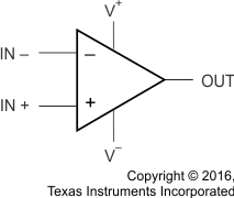
The amplifier's differential inputs consist of a non-inverting input (+IN) and an inverting input (–IN). The amplifier amplifies only the difference in voltage between the two inputs, which is called the differential input voltage. The output voltage of the op-amp VOUT is given by Equation 1:
where
- AOL is the open-loop gain of the amplifier, typically around 120 dB (1,000,000x, or 1,000,000 Volts per microvolt).
7.4 Device Functional Modes
7.4.1 Negative-Rail Sensing Input
The input common-mode voltage range of the LPV81x extends from (V-) to (V+) – 0.9 V. In this range, low offset can be expected with a minimum of 77dB CMRR. The LPV81x is protected from output "inversions" or "reversals".
7.4.2 Rail to Rail Output Stage
The LPV81x output voltage swings 3.5 mV from rails at 1.8 V supply, which provides the maximum possible dynamic range at the output. This is particularly important when operating on low supply voltages.
The LPV81x Maximum Output Voltage Swing graph defines the maximum swing possible under a particular output load.
7.4.3 Design Optimization for Nanopower Operation
When designing for ultra-low power, choose system feedback components carefully. To minimize quiescent current consumption, select large-value feedback resistors. Any large resistors will react with stray capacitance in the circuit and the input capacitance of the operational amplifier. These parasitic RC combinations can affect the stability of the overall system. A feedback capacitor may be required to assure stability and limit overshoot or gain peaking.
When possible, use AC coupling and AC feedback to reduce static current draw through the feedback elements. Use film or ceramic capacitors since large electrolytics may have large static leakage currents in the nanoamps.
7.4.4 Driving Capacitive Load
The LPV81x is internally compensated for stable unity gain operation, with a 8 kHz typical gain bandwidth. However, the unity gain follower is the most sensitive configuration to capacitive load. The combination of a capacitive load placed directly on the output of an amplifier along with the amplifier’s output impedance creates a phase lag, which reduces the phase margin of the amplifier. If the phase margin is significantly reduced, the response will be under damped which causes peaking in the transfer and, when there is too much peaking, the op amp might start oscillating.
In order to drive heavy (>50pF) capacitive loads, an isolation resistor, RISO, should be used, as shown in Figure 42. By using this isolation resistor, the capacitive load is isolated from the amplifier’s output. The larger the value of RISO, the more stable the amplifier will be. If the value of RISO is sufficiently large, the feedback loop will be stable, independent of the value of CL. However, larger values of RISO result in reduced output swing and reduced output current drive. The recommended value for RISO is 30-50kΩ.
 Figure 42. Resistive Isolation Of Capacitive Load