SLLS636N December 2004 – January 2015 MC33063A , MC34063A
PRODUCTION DATA.
- 1 Features
- 2 Description
- 3 Simplified Schematic
- 4 Revision History
- 5 Pin Configuration and Functions
-
6 Specifications
- 6.1 Absolute Maximum Ratings
- 6.2 ESD Ratings
- 6.3 Recommended Operating Conditions
- 6.4 Thermal Information
- 6.5 Electrical Characteristics—Oscillator
- 6.6 Electrical Characteristics—Output Switch
- 6.7 Electrical Characteristics—Comparator
- 6.8 Electrical Characteristics—Total Device
- 6.9 Typical Characteristics
- 7 Detailed Description
- 8 Application and Implementation
- 9 Power Supply Recommendations
- 10Layout
- 11Device and Documentation Support
- 12Mechanical, Packaging, and Orderable Information
Package Options
Mechanical Data (Package|Pins)
Thermal pad, mechanical data (Package|Pins)
- DRJ|8
Orderable Information
7 Detailed Description
7.1 Overview
The MC33063A and MC34063A devices are easy-to-use ICs containing all the primary circuitry needed for building simple DC-DC converters. These devices primarily consist of an internal temperature-compensated reference, a comparator, an oscillator, a PWM controller with active current limiting, a driver, and a high-current output switch. Thus, the devices require minimal external components to build converters in the boost, buck, and inverting topologies.
The MC33063A device is characterized for operation from –40°C to 85°C, while the MC34063A device is characterized for operation from 0°C to 70°C.
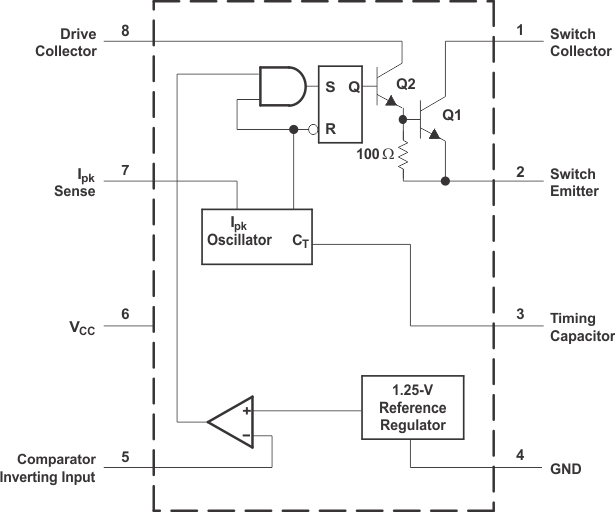
7.2 Functional Block Diagram
7.3 Feature Description
- Wide Input Voltage Range: 3 V to 40 V
- High Output Switch Current: Up to 1.5 A
- Adjustable Output Voltage
- Oscillator Frequency Up to 100 kHz
- Precision Internal Reference: 2%
- Short-Circuit Current Limiting
- Low Standby Current
7.4 Device Functional Modes
7.4.1 Standard operation
Based on the application, the device can be configured in multiple different topologies. See the Application and Implementation section for how to configure the device in several different operating modes.