SLLS636N December 2004 – January 2015 MC33063A , MC34063A
PRODUCTION DATA.
- 1 Features
- 2 Description
- 3 Simplified Schematic
- 4 Revision History
- 5 Pin Configuration and Functions
-
6 Specifications
- 6.1 Absolute Maximum Ratings
- 6.2 ESD Ratings
- 6.3 Recommended Operating Conditions
- 6.4 Thermal Information
- 6.5 Electrical Characteristics—Oscillator
- 6.6 Electrical Characteristics—Output Switch
- 6.7 Electrical Characteristics—Comparator
- 6.8 Electrical Characteristics—Total Device
- 6.9 Typical Characteristics
- 7 Detailed Description
- 8 Application and Implementation
- 9 Power Supply Recommendations
- 10Layout
- 11Device and Documentation Support
- 12Mechanical, Packaging, and Orderable Information
Package Options
Mechanical Data (Package|Pins)
Thermal pad, mechanical data (Package|Pins)
- DRJ|8
Orderable Information
8 Application and Implementation
NOTE
Information in the following applications sections is not part of the TI component specification, and TI does not warrant its accuracy or completeness. TI’s customers are responsible for determining suitability of components for their purposes. Customers should validate and test their design implementation to confirm system functionality.
8.1 Application Information
8.1.1 External Switch Configurations for Higher Peak Current
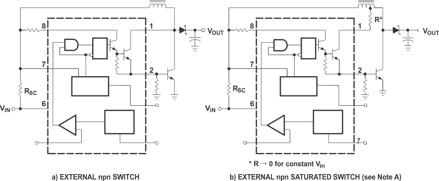
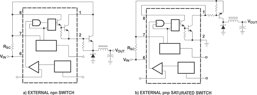 Figure 6. Buck Regulator Connections for IC Peak Greater Than 1.5 A
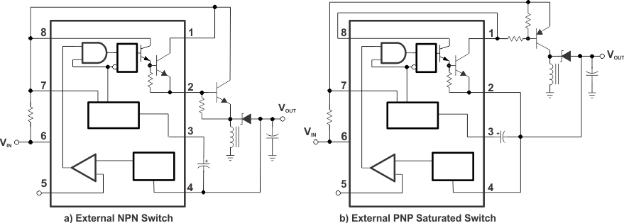 Figure 7. Inverting Regulator Connections for IC Peak Greater Than 1.5 A
8.2 Typical Application
8.2.1 Voltage-Inverting Converter Application
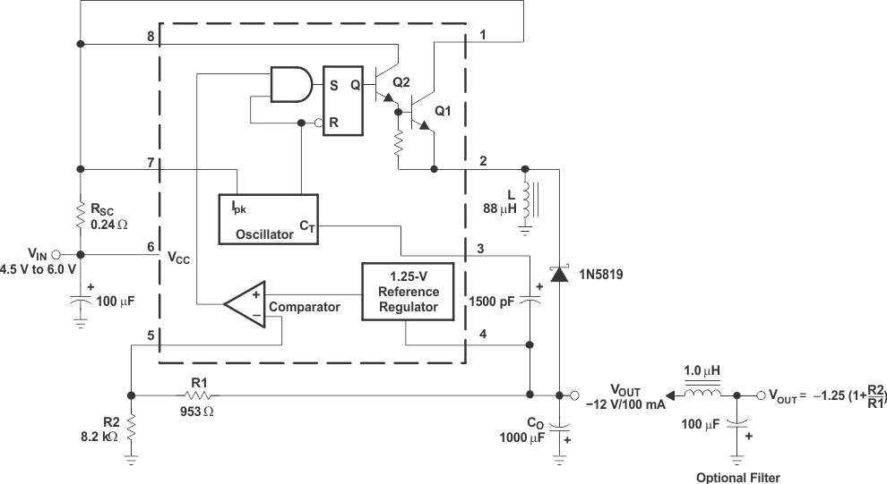 Figure 8. Voltage-Inverting Converter
8.2.1.1 Design Requirements
The user must determine the following desired parameters:
Vsat = Saturation voltage of the output switch
VF = Forward voltage drop of the chosen output rectifier
The following power-supply parameters are set by the user:
Vin = Nominal input voltage
Vout = Desired output voltage
Iout = Desired output current
fmin = Minimum desired output switching frequency at the selected values of Vin and Iout
Vripple = Desired peak-to-peak output ripple voltage. The ripple voltage directly affects the line and load regulation and, thus, must be considered. In practice, the actual capacitor value should be larger than the calculated value, to account for the capacitor's equivalent series resistance and board layout.
8.2.1.2 Detailed Design Procedure
| CALCULATION | VOLTAGE INVERTING |
|---|---|
| ton/toff |  |
| (ton + toff) |  |
| toff |  |
| ton |  |
| CT |  |
| Ipk(switch) |  |
| RSC |  |
| L(min) |  |
| CO |  |
| Vout | 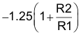
See Figure 8 |
8.2.1.3 Application Performance
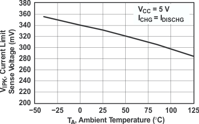 Figure 9. Current-Limit Sense Voltage vs Temperature
| TEST | CONDITIONS | RESULTS |
|---|---|---|
| Line regulation | VIN = 4.5 V to 6 V, IO = 100 mA | 3 mV ± 0.12% |
| Load regulation | VIN = 5 V, IO = 10 mA to 100 mA | 0.022 V ± 0.09% |
| Output ripple | VIN = 5 V, IO = 100 mA | 500 mVPP |
| Short-circuit current | VIN = 5 V, RL = 0.1 Ω | 910 mA |
| Efficiency | VIN = 5 V, IO = 100 mA | 62.2% |
| Output ripple with optional filter | VIN = 5 V, IO = 100 mA | 70 mVPP |
8.2.2 Step-Up Converter Application
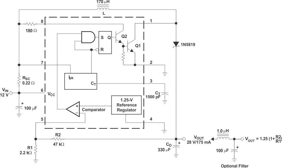 Figure 10. Step-Up Converter
8.2.2.1 Design Requirements
The user must determine the following desired parameters:
Vsat = Saturation voltage of the output switch
VF = Forward voltage drop of the chosen output rectifier
The following power-supply parameters are set by the user:
Vin = Nominal input voltage
Vout = Desired output voltage
Iout = Desired output current
fmin = Minimum desired output switching frequency at the selected values of Vin and Iout
Vripple = Desired peak-to-peak output ripple voltage. The ripple voltage directly affects the line and load regulation and, thus, must be considered. In practice, the actual capacitor value should be larger than the calculated value, to account for the capacitor's equivalent series resistance and board layout.
8.2.2.2 Detailed Design Procedure
| CALCULATION | STEP UP |
|---|---|
| ton/toff | 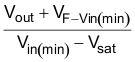 |
| (ton + toff) |  |
| toff |  |
| ton |  |
| CT |  |
| Ipk(switch) |  |
| RSC |  |
| L(min) |  |
| CO |  |
| Vout | 
See Figure 10 |
8.2.2.3 Application Performance
| TEST | CONDITIONS | RESULTS |
|---|---|---|
| Line regulation | VIN = 8 V to 16 V, IO = 175 mA | 30 mV ± 0.05% |
| Load regulation | VIN = 12 V, IO = 75 mA to 175 mA | 10 mV ± 0.017% |
| Output ripple | VIN = 12 V, IO = 175 mA | 400 mVPP |
| Efficiency | VIN = 12 V, IO = 175 mA | 87.7% |
| Output ripple with optional filter | VIN = 12 V, IO = 175 mA | 40 mVPP |
8.2.3 Step-Down Converter Application
 Figure 11. Step-Down Converter
8.2.3.1 Design Requirements
The user must determine the following desired parameters:
Vsat = Saturation voltage of the output switch
VF = Forward voltage drop of the chosen output rectifier
The following power-supply parameters are set by the user:
Vin = Nominal input voltage
Vout = Desired output voltage
Iout = Desired output current
fmin = Minimum desired output switching frequency at the selected values of Vin and Iout
Vripple = Desired peak-to-peak output ripple voltage. The ripple voltage directly affects the line and load regulation and, thus, must be considered. In practice, the actual capacitor value should be larger than the calculated value, to account for the capacitor's equivalent series resistance and board layout.
8.2.3.2 Detailed Design Procedure
| CALCULATION | STEP DOWN |
|---|---|
| ton/toff |  |
| (ton + toff) |  |
| toff |  |
| ton | 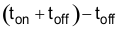 |
| CT |  |
| Ipk(switch) |  |
| RSC |  |
| L(min) | 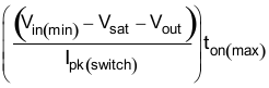 |
| CO | 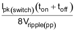 |
| Vout | 
See Figure 11 |
8.2.3.3 Application Performance
| TEST | CONDITIONS | RESULTS |
|---|---|---|
| Line regulation | VIN = 15 V to 25 V, IO = 500 mA | 12 mV ± 0.12% |
| Load regulation | VIN = 25 V, IO = 50 mA to 500 mA | 3 mV ± 0.03% |
| Output ripple | VIN = 25 V, IO = 500 mA | 120 mVPP |
| Short-circuit current | VIN = 25 V, RL = 0.1 Ω | 1.1 A |
| Efficiency | VIN = 25 V, IO = 500 mA | 83.7% |
| Output ripple with optional filter | VIN = 25 V, IO = 500 mA | 40 mVPP |