SLAS380F April 2004 – March 2022 MSP430FG437 , MSP430FG438 , MSP430FG439
PRODUCTION DATA
- 1 Features
- 2 Applications
- 3 Description
- 4 Functional Block Diagram
- 5 Revision History
- 6 Device Comparison
- 7 Terminal Configuration and Functions
-
8 Specifications
- 8.1 Absolute Maximum Ratings
- 8.2 Handling Ratings
- 8.3 Recommended Operating Conditions
- 8.4 Supply Current Into AVCC + DVCC Excluding External Current
- 8.5 Schmitt-Trigger Inputs – Ports P1 to P6, RST/NMI, JTAG (TCK, TMS, TDI/TCLK, TDO/TDI)
- 8.6 Inputs Px.y, TAx, TBx
- 8.7 Leakage Current – Ports P1 to P6
- 8.8 Outputs – Ports P1 to P6
- 8.9 Output Frequency
- 8.10 Typical Characteristics – Outputs
- 8.11 Wake-Up From LPM3
- 8.12 RAM
- 8.13 LCD
- 8.14 Comparator_A
- 8.15 Comparator_A Typical Characteristics
- 8.16 Power-On Reset (POR) and Brownout Reset (BOR)
- 8.17 Supply Voltage Supervisor (SVS) and Supply Voltage Monitor (SVM)
- 8.18 DCO
- 8.19 Crystal Oscillator, XT1 Oscillator
- 8.20 Crystal Oscillator, XT2 Oscillator
- 8.21 USART0
- 8.22 12-Bit ADC, Power Supply and Input Range Conditions
- 8.23 12-Bit ADC, External Reference
- 8.24 12-Bit ADC, Built-In Reference
- 8.25 12-Bit ADC, Timing Parameters
- 8.26 12-Bit ADC, Linearity Parameters
- 8.27 12-Bit ADC, Temperature Sensor and Built-In VMID
- 8.28 12-Bit DAC, Supply Specifications
- 8.29 12-Bit DAC, Linearity Specifications
- 8.30 12-Bit DAC, Output Specifications
- 8.31 12-Bit DAC, Reference Input Specifications
- 8.32 12-Bit DAC, Dynamic Specifications
- 8.33 12-Bit DAC, Dynamic Specifications (Continued)
- 8.34 Operational Amplifier (OA), Supply Specifications
- 8.35 Operational Amplifier (OA), Input/Output Specifications
- 8.36 Operational Amplifier (OA), Dynamic Specifications
- 8.37 OA Dynamic Specifications Typical Characteristics
- 8.38 Flash Memory
- 8.39 JTAG Interface
- 8.40 JTAG Fuse
-
9 Detailed Description
- 9.1 CPU
- 9.2 Instruction Set
- 9.3 Operating Modes
- 9.4 Interrupt Vector Addresses
- 9.5 Special Function Registers (SFRs)
- 9.6 Memory Organization
- 9.7 Bootstrap Loader (BSL)
- 9.8 Flash Memory
- 9.9
Peripherals
- 9.9.1 DMA Controller
- 9.9.2 Oscillator and System Clock
- 9.9.3 Brownout, Supply Voltage Supervisor
- 9.9.4 Digital I/O
- 9.9.5 Basic Timer1
- 9.9.6 LCD Drive
- 9.9.7 OA
- 9.9.8 Watchdog Timer (WDT)
- 9.9.9 USART0
- 9.9.10 Timer_A3
- 9.9.11 Timer_B3
- 9.9.12 Comparator_A
- 9.9.13 ADC12
- 9.9.14 DAC12
- 9.9.15 Peripheral File Map
- 9.10
Input/Output Schematics
- 9.10.1 Port P1, P1.0 to P1.5, Input/Output With Schmitt Trigger
- 9.10.2 Port P1, P1.6 and P1.7, Input/Output With Schmitt Trigger
- 9.10.3 Port P2, P2.0 and P2.4 to P2.5, Input/Output With Schmitt Trigger
- 9.10.4 Port P2, P2.1 to P2.3, Input/Output With Schmitt Trigger
- 9.10.5 Port P2, P2.6 and P2.7, Input/Output With Schmitt Trigger
- 9.10.6 Port P3, P3.0 to P3.3, Input/Output With Schmitt Trigger
- 9.10.7 Port P3, P3.4 to P3.7, Input/Output With Schmitt Trigger
- 9.10.8 Port P4, P4.0 to P4.5, Input/Output With Schmitt Trigger
- 9.10.9 Port P4, P4.6, Input/Output With Schmitt Trigger
- 9.10.10 Port P4, P4.7, Input/Output With Schmitt Trigger
- 9.10.11 Port P5, P5.0, Input/Output With Schmitt Trigger
- 9.10.12 Port P5, P5.1, Input/Output With Schmitt Trigger
- 9.10.13 Port P5, P5.2 to P5.4, Input/Output With Schmitt Trigger
- 9.10.14 Port P5, P5.5 to P5.7, Input/Output With Schmitt Trigger
- 9.10.15 Port P6, P6.0, P6.2, and P6.4, Input/Output With Schmitt Trigger
- 9.10.16 Port P6, P6.1, Input/Output With Schmitt Trigger
- 9.10.17 Port P6, P6.3, Input/Output With Schmitt Trigger
- 9.10.18 Port P6, P6.5, Input/Output With Schmitt Trigger
- 9.10.19 Port P6, P6.6, Input/Output With Schmitt Trigger
- 9.10.20 Port P6, P6.7, Input/Output With Schmitt Trigger
- 9.10.21 VeREF+/DAC0
- 9.10.22 JTAG Pins TMS, TCK, TDI/TCLK, TDO/TDI, Input/Output With Schmitt Trigger or Output
- 9.10.23 JTAG Fuse Check Mode
- 10Device and Documentation Support
- 11Mechanical Packaging and Orderable Information
Package Options
Mechanical Data (Package|Pins)
Thermal pad, mechanical data (Package|Pins)
Orderable Information
8.24 12-Bit ADC, Built-In Reference
over recommended operating free-air temperature range (unless otherwise noted)
| PARAMETER | TEST CONDITIONS | VCC | MIN | TYP | MAX | UNIT | |
|---|---|---|---|---|---|---|---|
| VREF+ | Positive built in reference voltage output | REF2_5V = 1 for 2.5 V, IVREF+max ≤ IVREF+ ≤ IVREF+min |
3 V | 2.4 | 2.5 | 2.6 | V |
| REF2_5V = 0 for 1.5 V, IVREF+max ≤ IVREF+ ≤ IVREF+min |
2.2 V, 3 V | 1.44 | 1.5 | 1.56 | |||
| AVCC(min) | AVCC minimum voltage, Positive built in reference active | REF2_5V = 0, IVREF+max ≤ IVREF+ ≤ IVREF+min |
2.2 | V | |||
| REF2_5V = 1, IVREF+min ≥ IVREF+ ≥ –0.5 mA |
2.8 | ||||||
| REF2_5V = 1, IVREF+min ≥ IVREF+ ≥ – 1 mA |
2.9 | ||||||
| IVREF+ | Load current out of VREF+ terminal | 2.2 V | 0.01 | –0.5 | mA | ||
| 3 V | 0.01 | –1 | |||||
| IL(VREF)+ | Load-current regulation, VREF+ terminal | IVREF+ = 500 µA ± 100 µA, Analog input voltage ≈ 0.75 V, REF2_5V = 0 |
2.2 V | ±2 | LSB | ||
| 3 V | ±2 | ||||||
| IVREF+ = 500 µA ± 100 µA, Analog input voltage ≈ 1.25 V, REF2_5V = 1 |
3 V | ±2 | LSB | ||||
| IDL(VREF)+ | Load current regulation, VREF+ terminal | IVREF+ = 100 µA → 900 µA, CVREF+ = 5 µF, ax ≈ 0.5 × VREF+, Error of conversion result ≤ 1 LSB |
3 V | 20 | ns | ||
| CVREF+ | Capacitance at pin VREF+(1) | REFON =1, 0 mA ≤ IVREF+ ≤ IVREF+max |
2.2 V, 3 V | 5 | 10 | µF | |
| TREF+ | Temperature coefficient of built-in reference | IVREF+ is a constant in the range of 0 mA ≤ IVREF+ ≤ 1 mA |
2.2 V, 3 V | ±100 | ppm/°C | ||
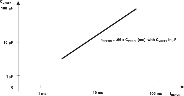
| tREFON | Settle time of internal reference voltage (see Figure 8-18 ) (2) | IVREF+ = 0.5 mA, CVREF+ = 10 µF, VREF+ = 1.5 V, VAVCC = 2.2 V |
17 | ms | |||
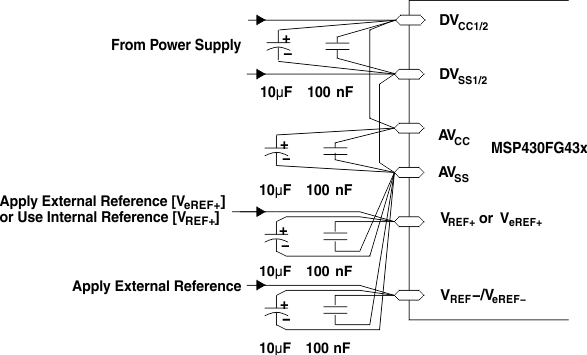
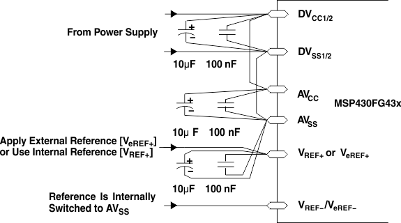
(1) The internal buffer operational amplifier and the accuracy specifications require an external capacitor. All INL and DNL tests uses two capacitors between pins VREF+ and AVSS and
VREF-–/VeREF– and AVSS: 10 µF tantalum and 100 nF ceramic.
(2) The condition is that the error in a conversion started after tREFON is less than ±0.5 LSB. The settling time depends on the external capacitive load.
 Figure 8-18 Typical Settling Time of Internal Reference tREFON vs External Capacitor on VREF+
 Figure 8-19 Supply Voltage and Reference Voltage Design VREF–/VeREF– External Supply
 Figure 8-20 Supply Voltage and Reference Voltage Design VREF–/VeREF– = AVSS, Internally Connected