SLAS734G April 2011 – April 2016 MSP430G2203 , MSP430G2233 , MSP430G2303 , MSP430G2333 , MSP430G2403 , MSP430G2433 , MSP430G2533
PRODUCTION DATA.
- 1Device Overview
- 2Revision History
- 3Device Comparison
- 4Terminal Configuration and Functions
-
5Specifications
- 5.1 Absolute Maximum Ratings
- 5.2 ESD Ratings
- 5.3 Recommended Operating Conditions
- 5.4 Active Mode Supply Current Into VCC Excluding External Current
- 5.5 Typical Characteristics, Active Mode Supply Current (Into VCC)
- 5.6 Low-Power Mode Supply Currents (Into VCC) Excluding External Current
- 5.7 Typical Characteristics, Low-Power Mode Supply Currents
- 5.8 Thermal Resistance Characteristics
- 5.9 Schmitt-Trigger Inputs, Ports Px
- 5.10 Leakage Current, Ports Px
- 5.11 Outputs, Ports Px
- 5.12 Output Frequency, Ports Px
- 5.13 Typical Characteristics - Outputs
- 5.14 Pin-Oscillator Frequency - Ports Px
- 5.15 Typical Characteristics - Pin-Oscillator Frequency
- 5.16 POR, BOR
- 5.17 Main DCO Characteristics
- 5.18 DCO Frequency
- 5.19 Calibrated DCO Frequencies, Tolerance
- 5.20 Wake-up Times From Lower-Power Modes (LPM3, LPM4)
- 5.21 Typical Characteristics, DCO Clock Wake-up Time From LPM3 or LPM4
- 5.22 Crystal Oscillator, XT1, Low-Frequency Mode
- 5.23 Internal Very-Low-Power Low-Frequency Oscillator (VLO)
- 5.24 Timer_A
- 5.25 USCI (UART Mode)
- 5.26 USCI (SPI Master Mode)
- 5.27 USCI (SPI Slave Mode)
- 5.28 USCI (I2C Mode)
- 5.29 10-Bit ADC, Power Supply and Input Range Conditions (MSP430G2x33 Only)
- 5.30 10-Bit ADC, Built-In Voltage Reference (MSP430G2x33 Only)
- 5.31 10-Bit ADC, External Reference (MSP430G2x33 Only)
- 5.32 10-Bit ADC, Timing Parameters (MSP430G2x33 Only)
- 5.33 10-Bit ADC, Linearity Parameters (MSP430G2x33 Only)
- 5.34 10-Bit ADC, Temperature Sensor and Built-In VMID (MSP430G2x33 Only)
- 5.35 Flash Memory
- 5.36 RAM
- 5.37 JTAG and Spy-Bi-Wire Interface
- 5.38 JTAG Fuse
-
6Detailed Description
- 6.1 CPU
- 6.2 Instruction Set
- 6.3 Operating Modes
- 6.4 Interrupt Vector Addresses
- 6.5 Special Function Registers (SFRs)
- 6.6 Memory Organization
- 6.7 Bootloader (BSL)
- 6.8 Flash Memory
- 6.9 Peripherals
- 6.10
I/O Port Diagrams
- 6.10.1 Port P1 Pin Diagram: P1.0 to P1.2, Input/Output With Schmitt Trigger
- 6.10.2 Port P1 Pin Diagram: P1.3, Input/Output With Schmitt Trigger
- 6.10.3 Port P1 Pin Diagram: P1.4, Input/Output With Schmitt Trigger
- 6.10.4 Port P1 Pin Diagram: P1.5 to P1.7, Input/Output With Schmitt Trigger
- 6.10.5 Port P2 Pin Diagram: P2.0 to P2.5, Input/Output With Schmitt Trigger
- 6.10.6 Port P2 Pin Diagram: P2.6, Input/Output With Schmitt Trigger
- 6.10.7 Port P2 Pin Diagram: P2.7, Input/Output With Schmitt Trigger
- 6.10.8 Port P3 Pin Diagram: P3.0 to P3.7, Input/Output With Schmitt Trigger (RHB and PW28 Package Only)
- 7Device and Documentation Support
- 8Mechanical, Packaging, and Orderable Information
Package Options
Mechanical Data (Package|Pins)
Thermal pad, mechanical data (Package|Pins)
- RHB|32
Orderable Information
4 Terminal Configuration and Functions
4.1 Pin Diagrams
Figure 4-1 shows the pinout for the MSP430G2x03 and MSP430G2x33 devices in the 20-pin N or PW package.

NOTE:
ADC10 is available on MSP430G2x33 devices only.NOTE:
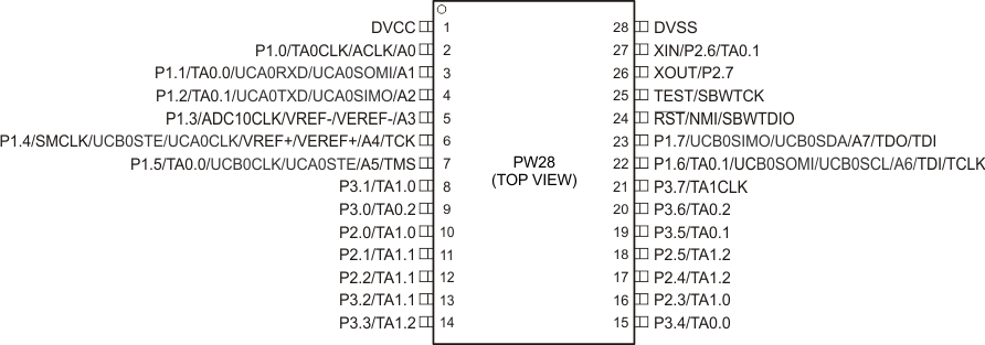
The pulldown resistors of port P3 should be enabled by setting P3REN.x = 1.Figure 4-2 shows the pinout for the MSP430G2x03 and MSP430G2x33 devices in the 28-pin PW package.

NOTE:
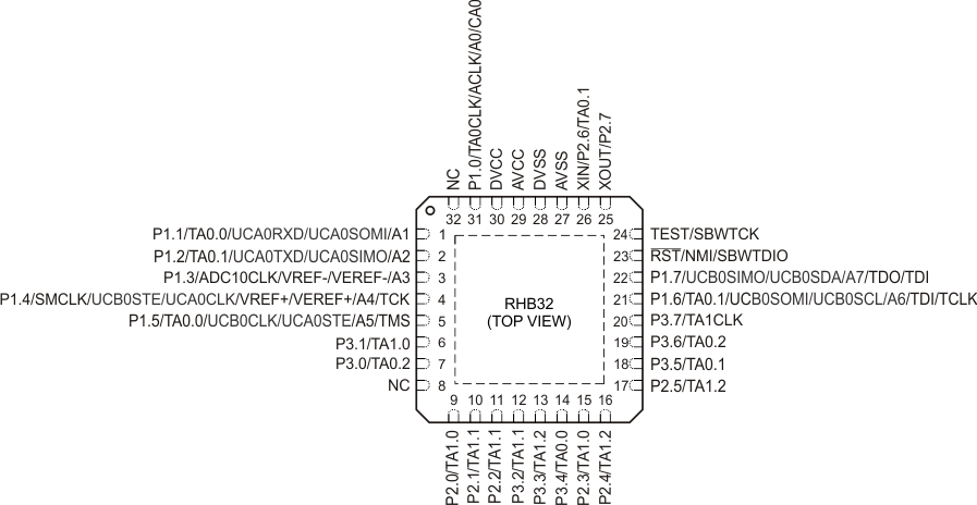
ADC10 is available on MSP430G2x33 devices only.Figure 4-3 shows the pinout for the MSP430G2x03 and MSP430G2x33 devices in the 32-pin RHB package.

NOTE:
ADC10 is available on MSP430G2x33 devices only.4.2 Signal Descriptions
Table 4-1 describes the signals.
Table 4-1 Terminal Functions
| TERMINAL | I/O | DESCRIPTION | |||
|---|---|---|---|---|---|
| NAME | NO. | ||||
| PW20, N20 | PW28 | RHB32 | |||
| P1.0/ | 2 | 2 | 31 | I/O | General-purpose digital I/O pin |
| TA0CLK/ | Timer0_A, clock signal TACLK input | ||||
| ACLK/ | ACLK signal output | ||||
| A0 | ADC10 analog input A0(1) | ||||
| P1.1/ | 3 | 3 | 1 | I/O | General-purpose digital I/O pin |
| TA0.0/ | Timer0_A, capture: CCI0A input, compare: Out0 output / BSL transmit | ||||
| UCA0RXD/ | USCI_A0 receive data input in UART mode | ||||
| UCA0SOMI/ | USCI_A0 slave data out/master in SPI mode | ||||
| A1 | ADC10 analog input A1(1) | ||||
| P1.2/ | 4 | 4 | 2 | I/O | General-purpose digital I/O pin |
| TA0.1/ | Timer0_A, capture: CCI1A input, compare: Out1 output | ||||
| UCA0TXD/ | USCI_A0 transmit data output in UART mode | ||||
| UCA0SIMO/ | USCI_A0 slave data in/master out in SPI mode | ||||
| A2 | ADC10 analog input A2(1) | ||||
| P1.3/ | 5 | 5 | 3 | I/O | General-purpose digital I/O pin |
| ADC10CLK/ | ADC10, conversion clock output(1) | ||||
| A3/ | ADC10 analog input A3(1) | ||||
| VREF-/VEREF- | ADC10 negative reference voltage (1) | ||||
| P1.4/ | 6 | 6 | 4 | I/O | General-purpose digital I/O pin |
| SMCLK/ | SMCLK signal output | ||||
| UCB0STE/ | USCI_B0 slave transmit enable | ||||
| UCA0CLK/ | USCI_A0 clock input/output | ||||
| A4/ | ADC10 analog input A4(1) | ||||
| VREF+/VEREF+ | ADC10 positive reference voltage(1) | ||||
| TCK | JTAG test clock, input terminal for device programming and test | ||||
| P1.5/ | 7 | 7 | 5 | I/O | General-purpose digital I/O pin |
| TA0.0/ | Timer0_A, compare: Out0 output / BSL receive | ||||
| UCB0CLK/ | USCI_B0 clock input/output | ||||
| UCA0STE/ | USCI_A0 slave transmit enable | ||||
| A5/ | ADC10 analog input A5(1) | ||||
| TMS | JTAG test mode select, input terminal for device programming and test | ||||
| P1.6/ | 14 | 22 | 21 | I/O | General-purpose digital I/O pin |
| TA0.1/ | Timer0_A, compare: Out1 output | ||||
| A6/ | ADC10 analog input A6(1) | ||||
| UCB0SOMI/ | USCI_B0 slave out/master in SPI mode, | ||||
| UCB0SCL/ | USCI_B0 SCL I2C clock in I2C mode | ||||
| TDI/TCLK | JTAG test data input or test clock input during programming and test | ||||
| P1.7/ | 15 | 23 | 22 | I/O | General-purpose digital I/O pin |
| A7/ | ADC10 analog input A7(1) | ||||
| UCB0SIMO/ | USCI_B0 slave in/master out in SPI mode | ||||
| UCB0SDA/ | USCI_B0 SDA I2C data in I2C mode | ||||
| TDO/TDI | JTAG test data output terminal or test data input during programming and test(3) | ||||
| P2.0/ | 8 | 10 | 9 | I/O | General-purpose digital I/O pin |
| TA1.0 | Timer1_A, capture: CCI0A input, compare: Out0 output | ||||
| P2.1/ | 9 | 11 | 10 | I/O | General-purpose digital I/O pin |
| TA1.1 | Timer1_A, capture: CCI1A input, compare: Out1 output | ||||
| P2.2/ | 10 | 12 | 11 | I/O | General-purpose digital I/O pin |
| TA1.1 | Timer1_A, capture: CCI1B input, compare: Out1 output | ||||
| P2.3/ | 11 | 16 | 15 | I/O | General-purpose digital I/O pin |
| TA1.0 | Timer1_A, capture: CCI0B input, compare: Out0 output | ||||
| P2.4/ | 12 | 17 | 16 | I/O | General-purpose digital I/O pin |
| TA1.2 | Timer1_A, capture: CCI2A input, compare: Out2 output | ||||
| P2.5/ | 13 | 18 | 17 | I/O | General-purpose digital I/O pin |
| TA1.2 | Timer1_A, capture: CCI2B input, compare: Out2 output | ||||
| XIN/ | 19 | 27 | 26 | I/O | Input terminal of crystal oscillator |
| P2.6/ | General-purpose digital I/O pin | ||||
| TA0.1 | Timer0_A, compare: Out1 output | ||||
| XOUT/ | 18 | 26 | 25 | I/O | Output terminal of crystal oscillator(2) |
| P2.7 | General-purpose digital I/O pin | ||||
| P3.0/ | - | 9 | 7 | I/O | General-purpose digital I/O pin |
| TA0.2 | Timer0_A, capture: CCI2A input, compare: Out2 output | ||||
| P3.1/ | - | 8 | 6 | I/O | General-purpose digital I/O pin |
| TA1.0 | Timer1_A, compare: Out0 output | ||||
| P3.2/ | - | 13 | 12 | I/O | General-purpose digital I/O pin |
| TA1.1 | Timer1_A, compare: Out1 output | ||||
| P3.3/ | - | 14 | 13 | I/O | General-purpose digital I/O |
| TA1.2 | Timer1_A, compare: Out2 output | ||||
| P3.4/ | - | 15 | 14 | I/O | General-purpose digital I/O |
| TA0.0 | Timer0_A, compare: Out0 output | ||||
| P3.5/ | - | 19 | 18 | I/O | General-purpose digital I/O |
| TA0.1 | Timer0_A, compare: Out1 output | ||||
| P3.6/ | - | 20 | 19 | I/O | General-purpose digital I/O |
| TA0.2 | Timer0_A, compare: Out2 output | ||||
| P3.7/ | - | 21 | 20 | I/O | General-purpose digital I/O |
| TA1CLK | Timer1_A, clock signal TACLK input | ||||
| RST/ | 16 | 24 | 23 | I | Reset |
| NMI/ | Nonmaskable interrupt input | ||||
| SBWTDIO | Spy-Bi-Wire test data input/output during programming and test | ||||
| TEST/ | 17 | 25 | 24 | I | Selects test mode for JTAG pins on Port 1. The device protection fuse is connected to TEST. |
| SBWTCK | Spy-Bi-Wire test clock input during programming and test | ||||
| AVCC | NA | NA | 29 | NA | Analog supply voltage |
| DVCC | 1 | 1 | 30 | NA | Digital supply voltage |
| DVSS | 20 | 28 | 27, 28 | NA | Ground reference |
| NC | NA | NA | 8, 32 | NA | Not connected |
| QFN Pad | NA | NA | Pad | NA | QFN package pad connection to VSS recommended. |
(1) MSP430G2x33 devices only
(2) If XOUT/P2.7 is used as an input, excess current flows until P2SEL.7 is cleared. This is due to the oscillator output driver connection to this pad after reset.
(3) TDO or TDI is selected by JTAG instruction.