SLAS892C March 2013 – September 2014 MSP430G2444 , MSP430G2544 , MSP430G2744
PRODUCTION DATA.
- 1Device Overview
- 2Revision History
- 3Device Comparison
- 4Terminal Configuration and Functions
-
5Specifications
- 5.1 Absolute Maximum Ratings
- 5.2 Handling Ratings
- 5.3 Recommended Operating Conditions
- 5.4 Active Mode Supply Current (Into DVCC + AVCC) Excluding External Current
- 5.5 Typical Characteristics - Active-Mode Supply Current (Into DVCC + AVCC)
- 5.6 Low-Power-Mode Supply Currents (Into VCC ) Excluding External Current
- 5.7 Schmitt-Trigger Inputs (Ports P1, P2, P3, P4, and RST/NMI)
- 5.8 Leakage Current, Ports Px
- 5.9 Outputs, Ports Px
- 5.10 Output Frequency, Ports Px
- 5.11 Typical Characteristics - Outputs
- 5.12 POR and BOR
- 5.13 Typical Characteristics - POR and BOR
- 5.14 DCO Frequency
- 5.15 Calibrated DCO Frequencies, Tolerance
- 5.16 Wake-Up From Lower-Power Modes (LPM3, LPM4)
- 5.17 Typical Characteristics - DCO Clock Wake-Up Time From LPM3 or LPM4
- 5.18 DCO With External Resistor ROSC
- 5.19 Typical Characteristics - DCO With External Resistor ROSC
- 5.20 Crystal Oscillator LFXT1, Low-Frequency Mode
- 5.21 Internal Very-Low-Power Low-Frequency Oscillator (VLO)
- 5.22 Crystal Oscillator LFXT1, High-Frequency Mode
- 5.23 Typical Characteristics - LFXT1 Oscillator in HF Mode (XTS = 1)
- 5.24 Timer_A, Timer_B
- 5.25 USCI (UART Mode)
- 5.26 USCI (SPI Master Mode)
- 5.27 USCI (SPI Slave Mode)
- 5.28 USCI (I2C Mode)
- 5.29 10-Bit ADC, Power Supply and Input Range Conditions
- 5.30 10-Bit ADC, Built-In Voltage Reference
- 5.31 10-Bit ADC, External Reference
- 5.32 10-Bit ADC, Timing Parameters
- 5.33 10-Bit ADC, Linearity Parameters
- 5.34 10-Bit ADC, Temperature Sensor and Built-In VMID
- 5.35 Flash Memory
- 5.36 RAM
- 5.37 JTAG and Spy-Bi-Wire Interface
- 5.38 JTAG Fuse
-
6Detailed Description
- 6.1 CPU
- 6.2 Instruction Set
- 6.3 Operating Modes
- 6.4 Interrupt Vector Addresses
- 6.5 Special Function Registers
- 6.6 Memory Organization
- 6.7 Bootstrap Loader (BSL)
- 6.8 Flash Memory
- 6.9 Peripherals
- 6.10 Oscillator and System Clock
- 6.11 Brownout
- 6.12 Digital I/O
- 6.13 Watchdog Timer (WDT+)
- 6.14 Timer_A3
- 6.15 Timer_B3
- 6.16 Universal Serial Communications Interface (USCI)
- 6.17 ADC10
- 6.18 Peripheral File Map
- 6.19
Port Schematics
- 6.19.1 Port P1 Pin Schematic: P1.0 to P1.3, Input/Output With Schmitt Trigger
- 6.19.2 Port P1 Pin Schematic: P1.4 to P1.6, Input/Output With Schmitt Trigger and In-System Access Features
- 6.19.3 Port P1 Pin Schematic: P1.7, Input/Output With Schmitt Trigger and In-System Access Features
- 6.19.4 Port P2 Pin Schematic: P2.0, P2.2, Input/Output With Schmitt Trigger
- 6.19.5 Port P2 Pin Schematic: P2.1, Input/Output With Schmitt Trigger
- 6.19.6 Port P2 Pin Schematic: P2.3, Input/Output With Schmitt Trigger
- 6.19.7 Port P2 Pin Schematic: P2.4, Input/Output With Schmitt Trigger
- 6.19.8 Port P2 Pin Schematic: P2.5, Input/Output With Schmitt Trigger and External ROSC for DCO
- 6.19.9 Port P2 Pin Schematic: P2.6, Input/Output With Schmitt Trigger and Crystal Oscillator Input
- 6.19.10 Port P2 Pin Schematic: P2.7, Input/Output With Schmitt Trigger and Crystal Oscillator Output
- 6.19.11 Port P3 Pin Schematic: P3.0, Input/Output With Schmitt Trigger
- 6.19.12 Port P3 Pin Schematic: P3.1 to P3.5, Input/Output With Schmitt Trigger
- 6.19.13 Port P3 Pin Schematic: P3.6 to P3.7, Input/Output With Schmitt Trigger
- 6.19.14 Port P4 Pin Schematic: P4.0 to P4.2, Input/Output With Schmitt Trigger
- 6.19.15 Port P4 Pin Schematic: P4.3 to P4.4, Input/Output With Schmitt Trigger
- 6.19.16 Port P4 Pin Schematic: P4.5, Input/Output With Schmitt Trigger
- 6.19.17 Port P4 Pin Schematic: P4.6, Input/Output With Schmitt Trigger
- 6.19.18 Port P4 Pin Schematic: P4.7, Input/Output With Schmitt Trigger
- 6.19.19 JTAG Fuse Check Mode
-
7Device and Documentation Support
- 7.1 Device Support
- 7.2 Documentation Support
- 7.3 Related Links
- 7.4 Community Resources
- 7.5 Trademarks
- 7.6 Electrostatic Discharge Caution
- 7.7 Glossary
- 8Mechanical, Packaging, and Orderable Information
Package Options
Mechanical Data (Package|Pins)
Thermal pad, mechanical data (Package|Pins)
Orderable Information
1 Device Overview
1.1 Features
- Low Supply-Voltage Range: 1.8 V to 3.6 V
- Ultra-Low Power Consumption
- Active Mode: 270 µA at 1 MHz, 2.2 V
- Standby Mode: 1 µA
- Off Mode (RAM Retention): 0.1 µA
- Ultra-Fast Wakeup From Standby Mode in Less Than 1 µs
- 16-Bit RISC Architecture, 62.5-ns Instruction Cycle Time
- Basic Clock Module Configurations
- Internal Frequencies up to 16 MHz With Four Calibrated Frequencies
- Internal Very-Low-Power Low-Frequency (LF) Oscillator
- 32-kHz Crystal
- High-Frequency (HF) Crystal up to 16 MHz
- Resonator
- External Digital Clock Source
- External Resistor
- 16-Bit Timer_A With Three Capture/Compare Registers
- 16-Bit Timer_B With Three Capture/Compare Registers
- Universal Serial Communication Interface (USCI)
- Enhanced UART Supports Automatic Baud-Rate Detection (LIN)
- IrDA Encoder and Decoder
- Synchronous SPI
- I2C
- 10-Bit 200-ksps Analog-to-Digital Converter (ADC) With Internal Reference, Sample-and-Hold, Autoscan, and Data Transfer Controller
- Brownout Detector
- Serial Onboard Programming, No External Programming Voltage Needed, Programmable Code Protection by Security Fuse
- Bootstrap Loader (BSL)
- On-Chip Emulation Module
- Family Members
- MSP430G2444
- 8KB + 256B Flash Memory
- 512B RAM
- MSP430G2544
- 16KB + 256B Flash Memory
- 512B RAM
- MSP430G2744
- 32KB + 256B Flash Memory
- 1KB RAM
- MSP430G2444
- Section 3 Summarizes the Available Family Members
- Package Options
- TSSOP: 38 Pin (DA)
- QFN: 40 Pin (RHA)
- DSBGA: 49 Pin (YFF)
- PDIP: 40 Pin (N) Available in Sampling Quantities as PMS430G2744IN40
- For Complete Module Descriptions, See the MSP430x2xx Family User's Guide (SLAU144)
1.2 Applications
- Sensor Systems
- Radio-Frequency Sensor Front End
1.3 Description
The Texas Instruments MSP430™ family of ultra-low-power microcontrollers consists of several devices featuring different sets of peripherals targeted for various applications. The architecture, combined with five low-power modes, is optimized to achieve extended battery life in portable measurement applications. The device features a powerful 16-bit RISC CPU, 16-bit registers, and constant generators that contribute to maximum code efficiency. The digitally controlled oscillator (DCO) allows the device to wake up from low-power modes to active mode in less than 1 µs.
The MSP430G2x44 series is an ultra-low-power mixed-signal microcontroller with two built-in 16-bit timers, a universal serial communication interface (USCI), 10-bit analog-to-digital converter (ADC) with integrated reference and data transfer controller (DTC), and 32 I/O pins.
Typical applications include sensor systems that capture analog signals, convert them to digital values, and then process the data for display or for transmission to a host system. Stand-alone radio-frequency (RF) sensor front ends are another area of application.
Device Information(1)
| PART NUMBER | PACKAGE | BODY SIZE(2) |
|---|---|---|
| MSP430G2744DA | TSSOP (38) | 12.5 mm x 6.2 mm |
| MSP430G2744RHA | VQFN (40) | 6 mm xm 6 mm |
| MSP430G2744YFF | DSBGA (49) | 3.1 mm x 3.1 mm |
| PMS430G2744N | PDIP (40) | 52.46 mm x 13.71 mm |
1.4 Functional Block Diagram
Figure 1-1 shows the functional block diagram of the MSP430G2x44 devices.
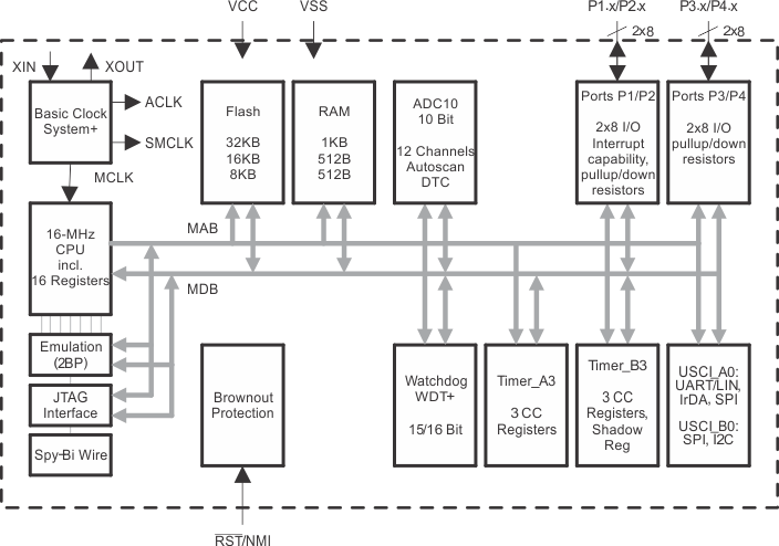 Figure 1-1 Functional Block Diagram