SLAS892C March 2013 – September 2014 MSP430G2444 , MSP430G2544 , MSP430G2744
PRODUCTION DATA.
- 1Device Overview
- 2Revision History
- 3Device Comparison
- 4Terminal Configuration and Functions
-
5Specifications
- 5.1 Absolute Maximum Ratings
- 5.2 Handling Ratings
- 5.3 Recommended Operating Conditions
- 5.4 Active Mode Supply Current (Into DVCC + AVCC) Excluding External Current
- 5.5 Typical Characteristics - Active-Mode Supply Current (Into DVCC + AVCC)
- 5.6 Low-Power-Mode Supply Currents (Into VCC ) Excluding External Current
- 5.7 Schmitt-Trigger Inputs (Ports P1, P2, P3, P4, and RST/NMI)
- 5.8 Leakage Current, Ports Px
- 5.9 Outputs, Ports Px
- 5.10 Output Frequency, Ports Px
- 5.11 Typical Characteristics - Outputs
- 5.12 POR and BOR
- 5.13 Typical Characteristics - POR and BOR
- 5.14 DCO Frequency
- 5.15 Calibrated DCO Frequencies, Tolerance
- 5.16 Wake-Up From Lower-Power Modes (LPM3, LPM4)
- 5.17 Typical Characteristics - DCO Clock Wake-Up Time From LPM3 or LPM4
- 5.18 DCO With External Resistor ROSC
- 5.19 Typical Characteristics - DCO With External Resistor ROSC
- 5.20 Crystal Oscillator LFXT1, Low-Frequency Mode
- 5.21 Internal Very-Low-Power Low-Frequency Oscillator (VLO)
- 5.22 Crystal Oscillator LFXT1, High-Frequency Mode
- 5.23 Typical Characteristics - LFXT1 Oscillator in HF Mode (XTS = 1)
- 5.24 Timer_A, Timer_B
- 5.25 USCI (UART Mode)
- 5.26 USCI (SPI Master Mode)
- 5.27 USCI (SPI Slave Mode)
- 5.28 USCI (I2C Mode)
- 5.29 10-Bit ADC, Power Supply and Input Range Conditions
- 5.30 10-Bit ADC, Built-In Voltage Reference
- 5.31 10-Bit ADC, External Reference
- 5.32 10-Bit ADC, Timing Parameters
- 5.33 10-Bit ADC, Linearity Parameters
- 5.34 10-Bit ADC, Temperature Sensor and Built-In VMID
- 5.35 Flash Memory
- 5.36 RAM
- 5.37 JTAG and Spy-Bi-Wire Interface
- 5.38 JTAG Fuse
-
6Detailed Description
- 6.1 CPU
- 6.2 Instruction Set
- 6.3 Operating Modes
- 6.4 Interrupt Vector Addresses
- 6.5 Special Function Registers
- 6.6 Memory Organization
- 6.7 Bootstrap Loader (BSL)
- 6.8 Flash Memory
- 6.9 Peripherals
- 6.10 Oscillator and System Clock
- 6.11 Brownout
- 6.12 Digital I/O
- 6.13 Watchdog Timer (WDT+)
- 6.14 Timer_A3
- 6.15 Timer_B3
- 6.16 Universal Serial Communications Interface (USCI)
- 6.17 ADC10
- 6.18 Peripheral File Map
- 6.19
Port Schematics
- 6.19.1 Port P1 Pin Schematic: P1.0 to P1.3, Input/Output With Schmitt Trigger
- 6.19.2 Port P1 Pin Schematic: P1.4 to P1.6, Input/Output With Schmitt Trigger and In-System Access Features
- 6.19.3 Port P1 Pin Schematic: P1.7, Input/Output With Schmitt Trigger and In-System Access Features
- 6.19.4 Port P2 Pin Schematic: P2.0, P2.2, Input/Output With Schmitt Trigger
- 6.19.5 Port P2 Pin Schematic: P2.1, Input/Output With Schmitt Trigger
- 6.19.6 Port P2 Pin Schematic: P2.3, Input/Output With Schmitt Trigger
- 6.19.7 Port P2 Pin Schematic: P2.4, Input/Output With Schmitt Trigger
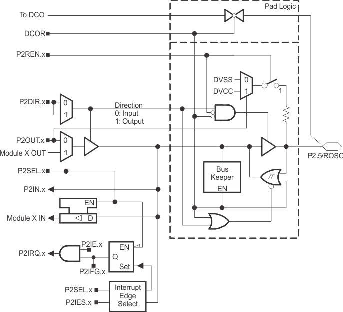
- 6.19.8 Port P2 Pin Schematic: P2.5, Input/Output With Schmitt Trigger and External ROSC for DCO
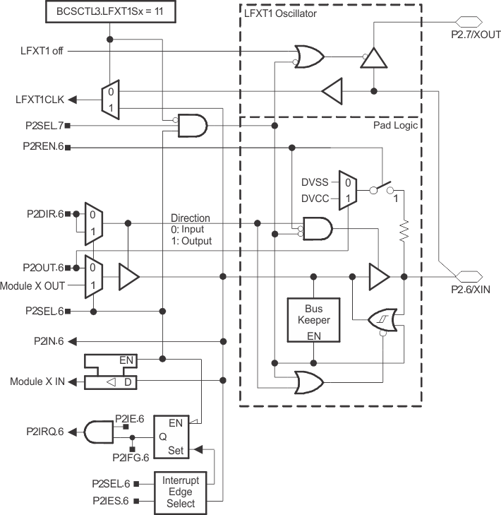
- 6.19.9 Port P2 Pin Schematic: P2.6, Input/Output With Schmitt Trigger and Crystal Oscillator Input
- 6.19.10 Port P2 Pin Schematic: P2.7, Input/Output With Schmitt Trigger and Crystal Oscillator Output
- 6.19.11 Port P3 Pin Schematic: P3.0, Input/Output With Schmitt Trigger
- 6.19.12 Port P3 Pin Schematic: P3.1 to P3.5, Input/Output With Schmitt Trigger
- 6.19.13 Port P3 Pin Schematic: P3.6 to P3.7, Input/Output With Schmitt Trigger
- 6.19.14 Port P4 Pin Schematic: P4.0 to P4.2, Input/Output With Schmitt Trigger
- 6.19.15 Port P4 Pin Schematic: P4.3 to P4.4, Input/Output With Schmitt Trigger
- 6.19.16 Port P4 Pin Schematic: P4.5, Input/Output With Schmitt Trigger
- 6.19.17 Port P4 Pin Schematic: P4.6, Input/Output With Schmitt Trigger
- 6.19.18 Port P4 Pin Schematic: P4.7, Input/Output With Schmitt Trigger
- 6.19.19 JTAG Fuse Check Mode
-
7Device and Documentation Support
- 7.1 Device Support
- 7.2 Documentation Support
- 7.3 Related Links
- 7.4 Community Resources
- 7.5 Trademarks
- 7.6 Electrostatic Discharge Caution
- 7.7 Glossary
- 8Mechanical, Packaging, and Orderable Information
Package Options
Mechanical Data (Package|Pins)
Thermal pad, mechanical data (Package|Pins)
Orderable Information
6 Detailed Description
6.1 CPU
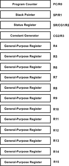
The MSP430™ CPU has a 16-bit RISC architecture that is highly transparent to the application. All operations, other than program-flow instructions, are performed as register operations in conjunction with seven addressing modes for source operand and four addressing modes for destination operand.
The CPU is integrated with 16 registers that provide reduced instruction execution time. The register-to-register operation execution time is one cycle of the CPU clock.
Four of the registers, R0 to R3, are dedicated as program counter, stack pointer, status register, and constant generator respectively. The remaining registers are general-purpose registers.
Peripherals are connected to the CPU using data, address, and control buses and can be handled with all instructions.
6.2 Instruction Set
The instruction set consists of 51 instructions with three formats and seven address modes. Each instruction can operate on word and byte data. Table 6-1 shows examples of the three types of instruction formats; Table 6-2 shows the address modes.
Table 6-1 Instruction Word Formats
| INSTRUCTION FORMAT | EXAMPLE | OPERATION |
|---|---|---|
| Dual operands, source-destination | ADD R4,R5 | R4 + R5 → R5 |
| Single operands, destination only | CALL R8 | PC → (TOS), R8 → PC |
| Relative jump, unconditional/conditional | JNE | Jump-on-equal bit = 0 |
Table 6-2 Address Mode Descriptions
| ADDRESS MODE | S(1) | D(2) | SYNTAX | EXAMPLE | OPERATION |
|---|---|---|---|---|---|
| Register | ✓ | ✓ | MOV Rs,Rd | MOV R10,R11 | R10 → R11 |
| Indexed | ✓ | ✓ | MOV X(Rn),Y(Rm) | MOV 2(R5),6(R6) | M(2+R5) → M(6+R6) |
| Symbolic (PC relative) | ✓ | ✓ | MOV EDE,TONI | M(EDE) → M(TONI) | |
| Absolute | ✓ | ✓ | MOV &MEM,&TCDAT | M(MEM) → M(TCDAT) | |
| Indirect | ✓ | MOV @Rn,Y(Rm) | MOV @R10,Tab(R6) | M(R10) → M(Tab+R6) | |
| Indirect autoincrement | ✓ | MOV @Rn+,Rm | MOV @R10+,R11 | M(R10) → R11 R10 + 2 → R10 |
|
| Immediate | ✓ | MOV #X,TONI | MOV #45,TONI | #45 → M(TONI) |
6.3 Operating Modes
The MSP430 microcontrollers have one active mode and five software-selectable low-power modes of operation. An interrupt event can wake up the device from any of the five low-power modes, service the request, and restore back to the low-power mode on return from the interrupt program.
The following six operating modes can be configured by software:
- Active mode (AM)
- All clocks are active.
- Low-power mode 0 (LPM0)
- CPU is disabled.
- ACLK and SMCLK remain active.
- MCLK is disabled.
- Low-power mode 1 (LPM1)
- CPU is disabled.
- ACLK and SMCLK remain active.
- MCLK is disabled.
- DCO dc-generator is disabled if DCO not used in active mode.
- Low-power mode 2 (LPM2)
- CPU is disabled.
- ACLK remains active.
- MCLK and SMCLK are disabled.
- DCO dc-generator remains enabled.
- Low-power mode 3 (LPM3)
- CPU is disabled.
- ACLK remains active.
- MCLK and SMCLK are disabled.
- DCO dc-generator is disabled.
- Low-power mode 4 (LPM4)
- CPU is disabled.
- ACLK, MCLK, and SMCLK are disabled.
- DCO dc-generator is disabled.
- Crystal oscillator is stopped.
6.4 Interrupt Vector Addresses
The interrupt vectors and the power-up starting address are located in the address range of 0FFFFh to 0FFC0h. The vector contains the 16-bit address of the appropriate interrupt handler instruction sequence.
If the reset vector (located at address 0FFFEh) contains 0FFFFh (for example, if flash is not programmed), the CPU goes into LPM4 immediately after power up.
Table 6-3 Interrupt Vector Addresses
| INTERRUPT SOURCE | INTERRUPT FLAG | SYSTEM INTERRUPT | WORD ADDRESS | PRIORITY |
|---|---|---|---|---|
| Power-up External reset Watchdog Flash key violation PC out-of-range(1) |
PORIFG RSTIFG WDTIFG KEYV(2) |
Reset | 0FFFEh | 31, highest |
| NMI Oscillator fault Flash memory access violation |
NMIIFG OFIFG ACCVIFG(2)(4) |
(non)-maskable, (non)-maskable, (non)-maskable |
0FFFCh | 30 |
| Timer_B3 | TBCCR0 CCIFG(3) | maskable | 0FFFAh | 29 |
| Timer_B3 | TBCCR1 and TBCCR2 CCIFGs, TBIFG(2)(3) | maskable | 0FFF8h | 28 |
| 0FFF6h | 27 | |||
| Watchdog Timer | WDTIFG | maskable | 0FFF4h | 26 |
| Timer_A3 | TACCR0 CCIFG(4) | maskable | 0FFF2h | 25 |
| Timer_A3 | TACCR1 CCIFG TACCR2 CCIFG TAIFG(2)(3) |
maskable | 0FFF0h | 24 |
| USCI_A0 or USCI_B0 Receive | UCA0RXIFG, UCB0RXIFG(2) | maskable | 0FFEEh | 23 |
| USCI_A0 or USCI_B0 Transmit | UCA0TXIFG, UCB0TXIFG(2) | maskable | 0FFECh | 22 |
| ADC10 | ADC10IFG(3) | maskable | 0FFEAh | 21 |
| 0FFE8h | 20 | |||
| I/O Port P2 (eight flags) |
P2IFG.0 to P2IFG.7(2)(3) | maskable | 0FFE6h | 19 |
| I/O Port P1 (eight flags) |
P1IFG.0 to P1IFG.7(2)(3) | maskable | 0FFE4h | 18 |
| 0FFE2h | 17 | |||
| 0FFE0h | 16 | |||
| (5) | 0FFDEh | 15 | ||
| (6) | 0FFDCh to 0FFC0h | 14 to 0, lowest |
Nonmaskable: neither the individual nor the general interrupt-enable bit will disable an interrupt event.
A 0AA55h at this location disables the BSL completely.
A zero (0h) disables the erasure of the flash if an invalid password is supplied.
6.5 Special Function Registers
Most interrupt and module enable bits are collected into the lowest address space. Special function register bits not allocated to a functional purpose are not physically present in the device. Simple software access is provided with this arrangement.
| Legend | ||
| rw | Bit can be read and written. | |
| rw-0, 1 | Bit can be read and written. It is Reset or Set by PUC. | |
| rw-(0), (1) | Bit can be read and written. It is Reset or Set by POR. | |
| SFR bit is not present in device. |
6.5.1 Interrupt Enable 1
| Address | 7 | 6 | 5 | 4 | 3 | 2 | 1 | 0 |
| 00h | ACCVIE | NMIIE | OFIE | WDTIE | ||||
| rw-0 | rw-0 | rw-0 | rw-0 |
| WDTIE | Watchdog timer interrupt enable. Inactive if watchdog mode is selected. Active if watchdog timer is configured in interval timer mode. |
| OFIE | Oscillator fault interrupt enable |
| NMIIE | (Non)maskable interrupt enable |
| ACCVIE | Flash access violation interrupt enable |
6.5.2 Interrupt Enable 2
| Address | 7 | 6 | 5 | 4 | 3 | 2 | 1 | 0 |
| 01h | UCB0TXIE | UCB0RXIE | UCA0TXIE | UCA0RXIE | ||||
| rw-0 | rw-0 | rw-0 | rw-0 |
| UCA0RXIE | USCI_A0 receive-interrupt enable |
| UCA0TXIE | USCI_A0 transmit-interrupt enable |
| UCB0RXIE | USCI_B0 receive-interrupt enable |
| UCB0TXIE | USCI_B0 transmit-interrupt enable |
6.5.3 Interrupt Flag Register 1
| Address | 7 | 6 | 5 | 4 | 3 | 2 | 1 | 0 |
| 02h | NMIIFG | RSTIFG | PORIFG | OFIFG | WDTIFG | |||
| rw-0 | rw-(0) | rw-(1) | rw-1 | rw-(0) |
| WDTIFG | Set on watchdog timer overflow (in watchdog mode) or security key violation. Reset on VCC power-up or a reset condition at RST/NMI pin in reset mode. |
| OFIFG | Flag set on oscillator fault |
| RSTIFG | External reset interrupt flag. Set on a reset condition at RST/NMI pin in reset mode. Reset on VCC power up. |
| PORIFG | Power-on reset interrupt flag. Set on VCC power up. |
| NMIIFG | Set via RST/NMI pin |
6.5.4 Interrupt Flag Register 2
| Address | 7 | 6 | 5 | 4 | 3 | 2 | 1 | 0 |
| 03h | UCB0TXIFG | UCB0RXIFG | UCA0TXIFG | UCA0RXIFG | ||||
| rw-1 | rw-0 | rw-1 | rw-0 |
| UCA0RXIFG | USCI_A0 receive interrupt flag |
| UCA0TXIFG | USCI_A0 transmit interrupt flag |
| UCB0RXIFG | USCI_B0 receive interrupt flag |
| UCB0TXIFG | USCI_B0 transmit interrupt flag |
6.6 Memory Organization
Table 6-4 Memory Organization
| MSP430G2444 | MSP430G2544 | MSP430G2744 | ||
| Memory Main: interrupt vector Main: code memory |
Size Flash Flash |
8KB Flash 0FFFFh-0FFC0h 0FFFFh-0E000h |
16KB Flash 0FFFFh-0FFC0h 0FFFFh-0C000h |
32KB Flash 0FFFFh-0FFC0h 0FFFFh-08000h |
| Information memory | Size Flash |
256 Byte 010FFh-01000h |
256 Byte 010FFh-01000h |
256 Byte 010FFh-01000h |
| Boot memory | Size ROM |
1KB 0FFFh-0C00h |
1KB 0FFFh-0C00h |
1KB 0FFFh-0C00h |
| RAM | Size | 512 Byte 03FFh-0200h |
512 Byte 03FFh-0200h |
1KB 05FFh-0200h |
| Peripherals | 16-bit 8-bit 8-bit SFR |
01FFh-0100h 0FFh-010h 0Fh-00h |
01FFh-0100h 0FFh-010h 0Fh-00h |
01FFh-0100h 0FFh-010h 0Fh-00h |
6.7 Bootstrap Loader (BSL)
The MSP430 bootstrap loader (BSL) enables users to program the flash memory or RAM using a UART serial interface. Access to the MSP430 memory via the BSL is protected by user-defined password. For complete description of the features of the BSL and its implementation, see the MSP430 Programming Via the Bootstrap Loader User’s Guide (SLAU319).
Table 6-5 BSL Function Pins
| BSL FUNCTION | DA PACKAGE PINS | RHA PACKAGE PINS | YFF PACKAGE PINS |
|---|---|---|---|
| Data transmit | 32 - P1.1 | 30 - P1.1 | G3 - P1.1 |
| Data receive | 10 - P2.2 | 8 - P2.2 | A5 - P2.2 |
6.8 Flash Memory
The flash memory can be programmed via the JTAG port, the bootstrap loader, or in-system by the CPU. The CPU can perform single-byte and single-word writes to the flash memory. Features of the flash memory include:
- Flash memory has n segments of main memory and four segments of information memory (A to D) of 64 bytes each. Each segment in main memory is 512 bytes in size.
- Segments 0 to n may be erased in one step, or each segment may be individually erased.
- Segments A to D can be erased individually, or as a group with segments 0 to n.
Segments A to D are also called information memory. - Segment A contains calibration data. After reset, segment A is protected against programming and erasing. It can be unlocked, but care should be taken not to erase this segment if the device-specific calibration data is required.
6.9 Peripherals
Peripherals are connected to the CPU through data, address, and control buses and can be handled using all instructions. For complete module descriptions, see the MSP430x2xx Family User's Guide (SLAU144).
6.10 Oscillator and System Clock
The clock system is supported by the basic clock module that includes support for a 32768-Hz watch crystal oscillator, an internal very-low-power low-frequency oscillator, an internal digitally-controlled oscillator (DCO), and a high-frequency crystal oscillator. The basic clock module is designed to meet the requirements of both low system cost and low power consumption. The internal DCO provides a fast turn-on clock source and stabilizes in less than 1 µs. The basic clock module provides the following clock signals:
- Auxiliary clock (ACLK), sourced from a 32768-Hz watch crystal, a high-frequency crystal, or the internal very-low-power LF oscillator.
- Main clock (MCLK), the system clock used by the CPU.
- Sub-Main clock (SMCLK), the sub-system clock used by the peripheral modules.
Table 6-6 DCO Calibration Data
(Provided From Factory in Flash Information Memory Segment A)
| DCO FREQUENCY | CALIBRATION REGISTER | SIZE | ADDRESS |
|---|---|---|---|
| 1 MHz | CALBC1_1MHZ | byte | 010FFh |
| CALDCO_1MHZ | byte | 010FEh | |
| 8 MHz | CALBC1_8MHZ | byte | 010FDh |
| CALDCO_8MHZ | byte | 010FCh | |
| 12 MHz | CALBC1_12MHZ | byte | 010FBh |
| CALDCO_12MHZ | byte | 010FAh | |
| 16 MHz | CALBC1_16MHZ | byte | 010F9h |
| CALDCO_16MHZ | byte | 010F8h |
6.11 Brownout
The brownout circuit is implemented to provide the proper internal reset signal to the device during power on and power off.
6.12 Digital I/O
There are four 8-bit I/O ports implemented—ports P1, P2, P3, and P4:
- All individual I/O bits are independently programmable.
- Any combination of input, output, and interrupt condition is possible.
- Edge-selectable interrupt input capability for all eight bits of port P1 and P2.
- Read and write access to port-control registers is supported by all instructions.
- Each I/O has an individually programmable pullup or pulldown resistor.
6.13 Watchdog Timer (WDT+)
The primary function of the WDT+ module is to perform a controlled system restart after a software problem occurs. If the selected time interval expires, a system reset is generated. If the watchdog function is not needed in an application, the module can be disabled or configured as an interval timer and can generate interrupts at selected time intervals.
6.14 Timer_A3
Timer_A3 is a 16-bit timer/counter with three capture/compare registers. Timer_A3 can support multiple capture/compares, PWM outputs, and interval timing. Timer_A3 also has extensive interrupt capabilities. Interrupts may be generated from the counter on overflow conditions and from each of the capture/compare registers.
Table 6-7 Timer_A3 Signal Connections
| INPUT PIN NUMBER | DEVICE INPUT SIGNAL | MODULE INPUT NAME | MODULE BLOCK | MODULE OUTPUT SIGNAL | OUTPUT PIN NUMBER | ||||||
|---|---|---|---|---|---|---|---|---|---|---|---|
| DA | N | RHA | YFF | DA | N | RHA | YFF | ||||
| 31 - P1.0 | 33 - P1.0 | 29 - P1.0 | F2 - P1.0 | TACLK | TACLK | Timer | NA | ||||
| ACLK | ACLK | ||||||||||
| SMCLK | SMCLK | ||||||||||
| 9 - P2.1 | 11 - P2.1 | 7 - P2.1 | B4 - P2.1 | TAINCLK | INCLK | ||||||
| 32 - P1.1 | 34 - P1.1 | 30 - P1.1 | G2 - P1.1 | TA0 | CCI0A | CCR0 | TA0 | 32 - P1.1 | 34 - P1.1 | 30 - P1.1 | G2 - P1.1 |
| 10 - P2.2 | 12 - P2.2 | 8 - P2.2 | A5 - P2.2 | TA0 | CCI0B | 10 - P2.2 | 12 - P2.2 | 8 - P2.2 | A5 - P2.2 | ||
| VSS | GND | 36 - P1.5 | 38 - P1.5 | 34 - P1.5 | E1 - P1.5 | ||||||
| VCC | VCC | ||||||||||
| 33 - P1.2 | 35 - P1.2 | 31 - P1.2 | E2 - P1.2 | TA1 | CCI1A | CCR1 | TA1 | 33 - P1.2 | 35 - P1.2 | 31 - P1.2 | E2 - P1.2 |
| 29 - P2.3 | 31 - P2.3 | 27 - P2.3 | F3 - P2.3 | TA1 | CCI1B | 29 - P2.3 | 31 - P2.3 | 27 - P2.3 | F3 - P2.3 | ||
| VSS | GND | 37 - P1.6 | 39 - P1.6 | 35 - P1.6 | E3 - P1.6 | ||||||
| VCC | VCC | ||||||||||
| 34 - P1.3 | 36 - P1.3 | 32 - P1.3 | G1 - P1.3 | TA2 | CCI2A | CCR2 | TA2 | 34 - P1.3 | 36 - P1.3 | 32 - P1.3 | G1 - P1.3 |
| ACLK (internal) | CCI2B | 30 - P2.4 | 32 - P2.4 | 28 - P2.4 | G3 - P2.4 | ||||||
| VSS | GND | 38 - P1.7 | 40 - P1.7 | 36 - P1.7 | D2 - P1.7 | ||||||
| VCC | VCC | ||||||||||
6.15 Timer_B3
Timer_B3 is a 16-bit timer/counter with three capture/compare registers. Timer_B3 can support multiple capture/compares, PWM outputs, and interval timing. Timer_B3 also has extensive interrupt capabilities. Interrupts may be generated from the counter on overflow conditions and from each of the capture/compare registers.
Table 6-8 Timer_B3 Signal Connections
| INPUT PIN NUMBER | DEVICE INPUT SIGNAL | MODULE INPUT NAME | MODULE BLOCK | MODULE OUTPUT SIGNAL | OUTPUT PIN NUMBER | ||||||
|---|---|---|---|---|---|---|---|---|---|---|---|
| DA | N | RHA | YFF | DA | N | RHA | YFF | ||||
| 24 - P4.7 | 26 - P4.7 | 22 - P4.7 | F5 - P4.7 | TBCLK | TBCLK | Timer | NA | ||||
| ACLK | ACLK | ||||||||||
| SMCLK | SMCLK | ||||||||||
| 24 - P4.7 | 26 - P4.7 | 22 - P4.7 | F5 - P4.7 | TBCLK | INCLK | ||||||
| 17 - P4.0 | 19 - P4.0 | 15 - P4.0 | D6 - P4.0 | TB0 | CCI0A | CCR0 | TB0 | 17 - P4.0 | 19 - P4.0 | 15 - P4.0 | D6 - P4.0 |
| 20 - P4.3 | 22 - P4.3 | 18 - P4.3 | E7 - P4.3 | TB0 | CCI0B | 20 - P4.3 | 22 - P4.3 | 18 - P4.3 | E7 - P4.3 | ||
| VSS | GND | ||||||||||
| VCC | VCC | ||||||||||
| 18 - P4.1 | 21 - P4.1 | 16 - P4.1 | D7 - P4.1 | TB1 | CCI1A | CCR1 | TB1 | 18 - P4.1 | 20 - P4.1 | 16 - P4.1 | D7 - P4.1 |
| 21 - P4.4 | 23 - P4.4 | 19 - P4.4 | F7 - P4.4 | TB1 | CCI1B | 21 - P4.4 | 23 - P4.4 | 19 - P4.4 | F7 - P4.4 | ||
| VSS | GND | ||||||||||
| VCC | VCC | ||||||||||
| 19 - P4.2 | 21 - P4.2 | 17 - P4.2 | E6 - P4.2 | TB2 | CCI2A | CCR2 | TB2 | 19 - P4.2 | 21 - P4.2 | 17 - P4.2 | E6 - P4.2 |
| ACLK (internal) | CCI2B | 22 - P4.5 | 24 - P4.5 | 20 - P4.5 | F6 - P4.5 | ||||||
| VSS | GND | ||||||||||
| VCC | VCC | ||||||||||
6.16 Universal Serial Communications Interface (USCI)
The USCI module is used for serial data communication. The USCI module supports synchronous communication protocols like SPI (3 or 4 pin), I2C and asynchronous communication protocols such as UART, enhanced UART with automatic baudrate detection (LIN), and IrDA.
USCI_A0 provides support for SPI (3 or 4 pin), UART, enhanced UART, and IrDA.
USCI_B0 provides support for SPI (3 or 4 pin) and I2C.
6.17 ADC10
The ADC10 module supports fast, 10-bit analog-to-digital conversions. The module implements a 10-bit SAR core, sample select control, reference generator and data transfer controller, or DTC, for automatic conversion result handling allowing ADC samples to be converted and stored without any CPU intervention.
6.18 Peripheral File Map
Table 6-9 lists the peripheral registers that have word access, and Table 6-10 lists the peripheral registers that have byte access.
Table 6-9 Peripherals With Word Access
| MODULE | REGISTER NAME | ACRONYM | ADDRESS OFFSET |
|---|---|---|---|
| ADC10 | ADC data transfer start address | ADC10SA | 1BCh |
| ADC memory | ADC10MEM | 1B4h | |
| ADC control register 1 | ADC10CTL1 | 1B2h | |
| ADC control register 0 | ADC10CTL0 | 1B0h | |
| ADC analog enable 0 | ADC10AE0 | 04Ah | |
| ADC analog enable 1 | ADC10AE1 | 04Bh | |
| ADC data transfer control register 1 | ADC10DTC1 | 049h | |
| ADC data transfer control register 0 | ADC10DTC0 | 048h | |
| Timer_B | Capture/compare register | TBCCR2 | 0196h |
| Capture/compare register | TBCCR1 | 0194h | |
| Capture/compare register | TBCCR0 | 0192h | |
| Timer_B register | TBR | 0190h | |
| Capture/compare control | TBCCTL2 | 0186h | |
| Capture/compare control | TBCCTL1 | 0184h | |
| Capture/compare control | TBCCTL0 | 0182h | |
| Timer_B control | TBCTL | 0180h | |
| Timer_B interrupt vector | TBIV | 011Eh | |
| Timer_A | Capture/compare register | TACCR2 | 0176h |
| Capture/compare register | TACCR1 | 0174h | |
| Capture/compare register | TACCR0 | 0172h | |
| Timer_A register | TAR | 0170h | |
| Capture/compare control | TACCTL2 | 0166h | |
| Capture/compare control | TACCTL1 | 0164h | |
| Capture/compare control | TACCTL0 | 0162h | |
| Timer_A control | TACTL | 0160h | |
| Timer_A interrupt vector | TAIV | 012Eh | |
| Flash Memory | Flash control 3 | FCTL3 | 012Ch |
| Flash control 2 | FCTL2 | 012Ah | |
| Flash control 1 | FCTL1 | 0128h | |
| Watchdog Timer+ | Watchdog/timer control | WDTCTL | 0120h |
Table 6-10 Peripherals With Byte Access
| MODULE | REGISTER NAME | ACRONYM | ADDRESS OFFSET |
|---|---|---|---|
| USCI_B0 | USCI_B0 transmit buffer | UCB0TXBUF | 06Fh |
| USCI_B0 receive buffer | UCB0RXBUF | 06Eh | |
| USCI_B0 status | UCB0STAT | 06Dh | |
| USCI_B0 bit rate control 1 | UCB0BR1 | 06Bh | |
| USCI_B0 bit rate control 0 | UCB0BR0 | 06Ah | |
| USCI_B0 control 1 | UCB0CTL1 | 069h | |
| USCI_B0 control 0 | UCB0CTL0 | 068h | |
| USCI_B0 I2C slave address | UCB0SA | 011Ah | |
| USCI_B0 I2C own address | UCB0OA | 0118h | |
| USCI_A0 | USCI_A0 transmit buffer | UCA0TXBUF | 067h |
| USCI_A0 receive buffer | UCA0RXBUF | 066h | |
| USCI_A0 status | UCA0STAT | 065h | |
| USCI_A0 modulation control | UCA0MCTL | 064h | |
| USCI_A0 baud rate control 1 | UCA0BR1 | 063h | |
| USCI_A0 baud rate control 0 | UCA0BR0 | 062h | |
| USCI_A0 control 1 | UCA0CTL1 | 061h | |
| USCI_A0 control 0 | UCA0CTL0 | 060h | |
| USCI_A0 IrDA receive control | UCA0IRRCTL | 05Fh | |
| USCI_A0 IrDA transmit control | UCA0IRTCTL | 05Eh | |
| USCI_A0 auto baud rate control | UCA0ABCTL | 05Dh | |
| Basic Clock System+ | Basic clock system control 3 | BCSCTL3 | 053h |
| Basic clock system control 2 | BCSCTL2 | 058h | |
| Basic clock system control 1 | BCSCTL1 | 057h | |
| DCO clock frequency control | DCOCTL | 056h | |
| Port P4 | Port P4 resistor enable | P4REN | 011h |
| Port P4 selection | P4SEL | 01Fh | |
| Port P4 direction | P4DIR | 01Eh | |
| Port P4 output | P4OUT | 01Dh | |
| Port P4 input | P4IN | 01Ch | |
| Port P3 | Port P3 resistor enable | P3REN | 010h |
| Port P3 selection | P3SEL | 01Bh | |
| Port P3 direction | P3DIR | 01Ah | |
| Port P3 output | P3OUT | 019h | |
| Port P3 input | P3IN | 018h | |
| Port P2 | Port P2 resistor enable | P2REN | 02Fh |
| Port P2 selection | P2SEL | 02Eh | |
| Port P2 interrupt enable | P2IE | 02Dh | |
| Port P2 interrupt edge select | P2IES | 02Ch | |
| Port P2 interrupt flag | P2IFG | 02Bh | |
| Port P2 direction | P2DIR | 02Ah | |
| Port P2 output | P2OUT | 029h | |
| Port P2 input | P2IN | 028h | |
| Port P1 | Port P1 resistor enable | P1REN | 027h |
| Port P1 selection | P1SEL | 026h | |
| Port P1 interrupt enable | P1IE | 025h | |
| Port P1 interrupt edge select | P1IES | 024h | |
| Port P1 interrupt flag | P1IFG | 023h | |
| Port P1 direction | P1DIR | 022h | |
| Port P1 output | P1OUT | 021h | |
| Port P1 input | P1IN | 020h | |
| Special Function | SFR interrupt flag 2 | IFG2 | 003h |
| SFR interrupt flag 1 | IFG1 | 002h | |
| SFR interrupt enable 2 | IE2 | 001h | |
| SFR interrupt enable 1 | IE1 | 000h |
6.19 Port Schematics
6.19.1 Port P1 Pin Schematic: P1.0 to P1.3, Input/Output With Schmitt Trigger
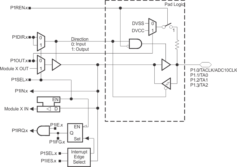
Table 6-11 Port P1 (P1.0 to P1.3) Pin Functions
| PIN NAME (P1.x) | x | FUNCTION | CONTROL BITS OR SIGNALS | |
|---|---|---|---|---|
| P1DIR.x | P1SEL.x | |||
| P1.0/TACLK/ADC10CLK | 0 | P1.0(1) | I: 0; O: 1 | 0 |
| Timer_A3.TACLK | 0 | 1 | ||
| ADC10CLK | 1 | 1 | ||
| P1.1/TA0 | 1 | P1.1(1) (I/O) | I: 0; O: 1 | 0 |
| Timer_A3.CCI0A | 0 | 1 | ||
| Timer_A3.TA0 | 1 | 1 | ||
| P1.2/TA1 | 2 | P1.2(1) (I/O) | I: 0; O: 1 | 0 |
| Timer_A3.CCI1A | 0 | 1 | ||
| Timer_A3.TA1 | 1 | 1 | ||
| P1.3/TA2 | 3 | P1.3(1) (I/O) | I: 0; O: 1 | 0 |
| Timer_A3.CCI2A | 0 | 1 | ||
| Timer_A3.TA2 | 1 | 1 | ||
6.19.2 Port P1 Pin Schematic: P1.4 to P1.6, Input/Output With Schmitt Trigger and In-System Access Features
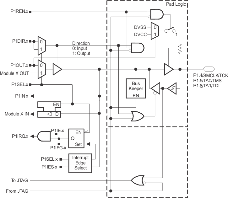
Table 6-12 Port P1 (P1.4 to P1.6) Pin Functions
| PIN NAME (P1.x) | x | FUNCTION | CONTROL BITS OR SIGNALS(2) | ||
|---|---|---|---|---|---|
| P1DIR.x | P1SEL.x | 4-Wire JTAG | |||
| P1.4/SMCLK/TCK | 4 | P1.4(1) (I/O) | I: 0; O: 1 | 0 | 0 |
| SMCLK | 1 | 1 | 0 | ||
| TCK | X | X | 1 | ||
| P1.5/TA0/TMS | 5 | P1.5(1) (I/O) | I: 0; O: 1 | 0 | 0 |
| Timer_A3.TA0 | 1 | 1 | 0 | ||
| TMS | X | X | 1 | ||
| P1.6/TA1/TDI/TCLK | 6 | P1.6(1) (I/O) | I: 0; O: 1 | 0 | 0 |
| Timer_A3.TA1 | 1 | 1 | 0 | ||
| TDI/TCLK(3) | X | X | 1 | ||
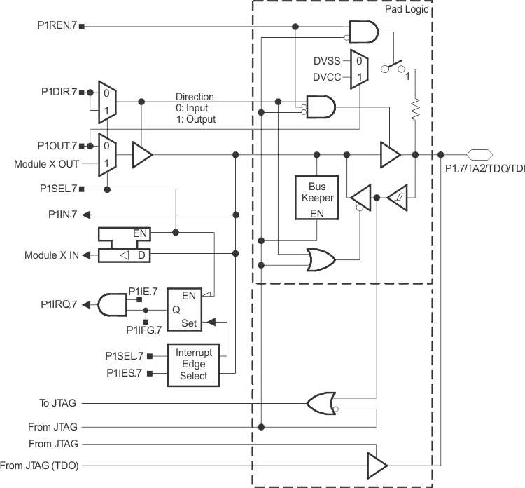
6.19.3 Port P1 Pin Schematic: P1.7, Input/Output With Schmitt Trigger and In-System Access Features
6.19.4 Port P2 Pin Schematic: P2.0, P2.2, Input/Output With Schmitt Trigger
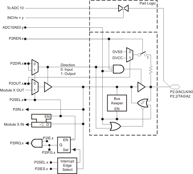
Table 6-14 Port P2 (P2.0, P2.2) Pin Functions
| Pin Name (P2.x) | x | y | FUNCTION | CONTROL BITS OR SIGNALS(1) | ||
|---|---|---|---|---|---|---|
| P2DIR.x | P2SEL.x | ADC10AE0.y | ||||
| P2.0/ACLK/A0 | 0 | 0 | P2.0(1) (I/O) | I: 0; O: 1 | 0 | 0 |
| ACLK | 1 | 1 | 0 | |||
| A0(2) | X | X | 1 | |||
| P2.2/TA0/A2 | 2 | 2 | P2.2(1) (I/O) | I: 0; O: 1 | 0 | 0 |
| Timer_A3.CCI0B | 0 | 1 | 0 | |||
| Timer_A3.TA0 | 1 | 1 | 0 | |||
| A2(2) | X | X | 1 | |||
6.19.5 Port P2 Pin Schematic: P2.1, Input/Output With Schmitt Trigger
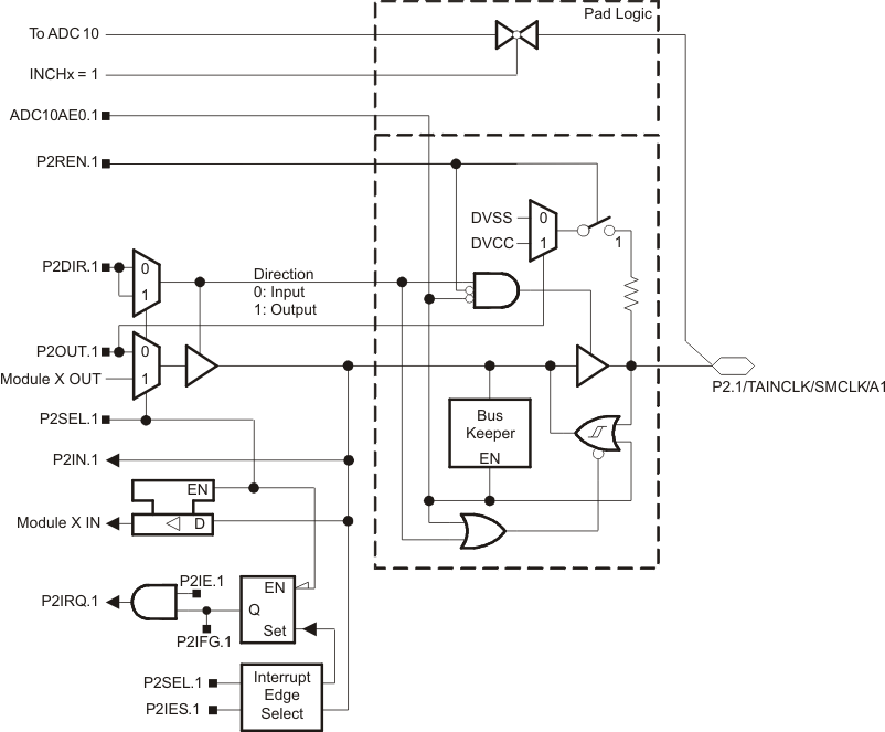
Table 6-15 Port P2 (P2.1) Pin Functions
| PIN NAME (P2.x) | x | y | FUNCTION | CONTROL BITS OR SIGNALS(1) | ||
|---|---|---|---|---|---|---|
| P2DIR.x | P2SEL.x | ADC10AE0.y | ||||
| P2.1/TAINCLK/ SMCLK/A1 | 1 | 1 | P2.1(2) (I/O) | I: 0; O: 1 | 0 | 0 |
| Timer_A3.INCLK | 0 | 1 | 0 | |||
| SMCLK | 1 | 1 | 0 | |||
| A1(3) | X | X | 1 | |||
6.19.6 Port P2 Pin Schematic: P2.3, Input/Output With Schmitt Trigger
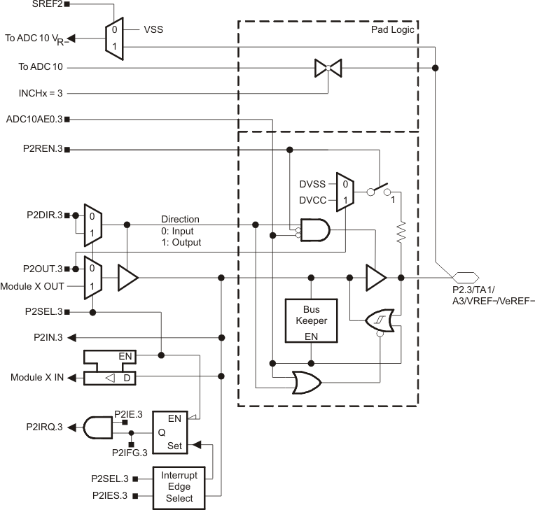
Table 6-16 Port P2 (P2.3) Pin Functions
| PIN NAME (P2.x) | x | y | FUNCTION | CONTROL BITS OR SIGNALS(1) | ||
|---|---|---|---|---|---|---|
| P2DIR.x | P2SEL.x | ADC10AE0.y | ||||
| P2.3/TA1/A3/ VREF-/VeREF- | 3 | 3 | P2.3(2) (I/O) | I: 0; O: 1 | 0 | 0 |
| Timer_A3.CCI1B | 0 | 1 | 0 | |||
| Timer_A3.TA1 | 1 | 1 | 0 | |||
| A3/VREF-/VeREF-(3) | X | X | 1 | |||
6.19.7 Port P2 Pin Schematic: P2.4, Input/Output With Schmitt Trigger
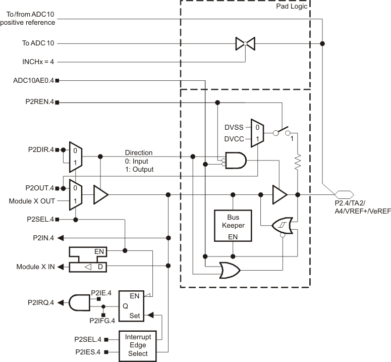
Table 6-17 Port P2 (P2.4) Pin Functions
| PIN NAME (P2.x) | x | y | FUNCTION | CONTROL BITS OR SIGNALS(1) | ||
|---|---|---|---|---|---|---|
| P2DIR.x | P2SEL.x | ADC10AE0.y | ||||
| P2.4/TA2/A4/ VREF+/VeREF+ | 4 | 4 | P2.4(2) (I/O) | I: 0; O: 1 | 0 | 0 |
| Timer_A3.TA2 | 1 | 1 | 0 | |||
| A4/VREF+/VeREF+(3) | X | X | 1 | |||
6.19.8 Port P2 Pin Schematic: P2.5, Input/Output With Schmitt Trigger and External ROSC for DCO
6.19.9 Port P2 Pin Schematic: P2.6, Input/Output With Schmitt Trigger and Crystal Oscillator Input
6.19.10 Port P2 Pin Schematic: P2.7, Input/Output With Schmitt Trigger and Crystal Oscillator Output
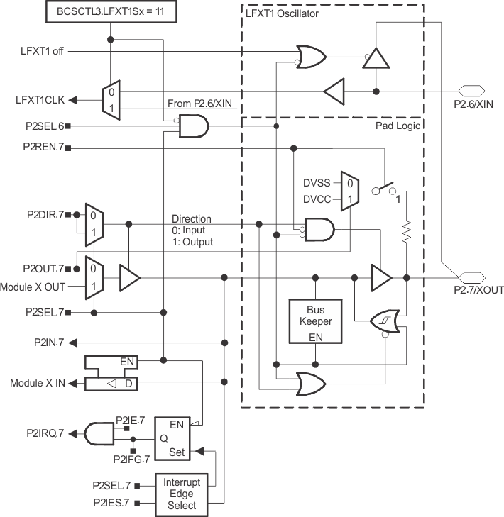
Table 6-20 Port P2 (P2.7) Pin Functions
| PIN NAME (P2.x) | x | FUNCTION | CONTROL BITS OR SIGNALS(1) | |
|---|---|---|---|---|
| P2DIR.x | P2SEL.x | |||
| XOUT/P2.7 | 7 | P2.7 (I/O) | I: 0; O: 1 | 0 |
| XOUT(2)(3) | X | 1 | ||
6.19.11 Port P3 Pin Schematic: P3.0, Input/Output With Schmitt Trigger
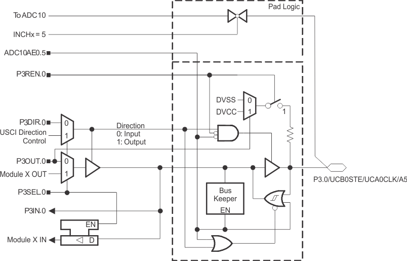
Table 6-21 Port P3 (P3.0) Pin Functions
| PIN NAME (P1.x) | x | y | FUNCTION | CONTROL BITS OR SIGNALS(1) | ||
|---|---|---|---|---|---|---|
| P3DIR.x | P3SEL.x | ADC10AE0.y | ||||
| P3.0/UCB0STE/ UCA0CLK/A5 | 0 | 5 | P3.0(2) (I/O) | I: 0; O: 1 | 0 | 0 |
| UCB0STE/UCA0CLK(3)(4) | X | 1 | 0 | |||
| A5(5) | X | X | 1 | |||
6.19.12 Port P3 Pin Schematic: P3.1 to P3.5, Input/Output With Schmitt Trigger
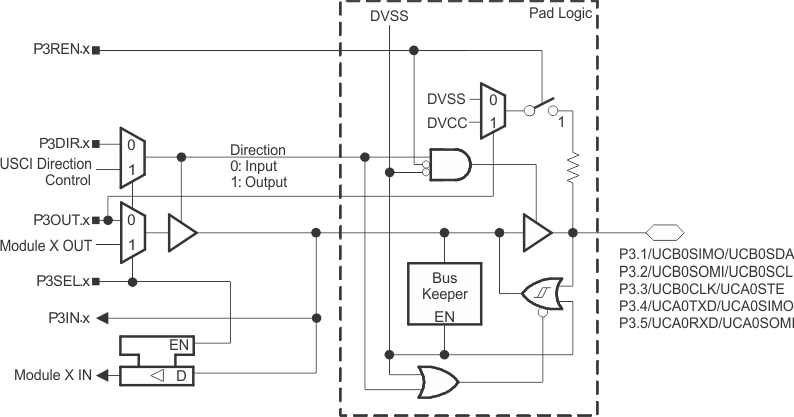
Table 6-22 Port P3 (P3.1 to P3.5) Pin Functions
| PIN NAME (P3.x) | x | FUNCTION | CONTROL BITS OR SIGNALS(1) | |
|---|---|---|---|---|
| P3DIR.x | P3SEL.x | |||
| P3.1/UCB0SIMO/UCB0SDA | 1 | P3.1(2) (I/O) | I: 0; O: 1 | 0 |
| UCB0SIMO/UCB0SDA(3) | X | 1 | ||
| P3.2/UCB0SOMI/UCB0SCL | 2 | P3.2(2) (I/O) | I: 0; O: 1 | 0 |
| UCB0SOMI/UCB0SCL(3) | X | 1 | ||
| P3.3/UCB0CLK/UCA0STE | 3 | P3.3(2) (I/O) | I: 0; O: 1 | 0 |
| UCB0CLK/UCA0STE(3)(4) | X | 1 | ||
| P3.4/UCA0TXD/UCA0SIMO | 4 | P3.4(2) (I/O) | I: 0; O: 1 | 0 |
| UCA0TXD/UCA0SIMO(3) | X | 1 | ||
| P3.5/UCA0RXD/UCA0SOMI | 5 | P3.5(2) (I/O) | I: 0; O: 1 | 0 |
| UCA0RXD/UCA0SOMI(3) | X | 1 | ||
6.19.13 Port P3 Pin Schematic: P3.6 to P3.7, Input/Output With Schmitt Trigger
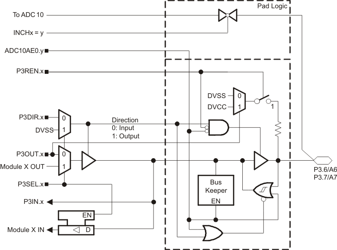
Table 6-23 Port P3 (P3.6, P3.7) Pin Functions
| PIN NAME (P3.x) | x | y | FUNCTION | CONTROL BITS OR SIGNALS(1) | ||
|---|---|---|---|---|---|---|
| P3DIR.x | P3SEL.x | ADC10AE0.y | ||||
| P3.6/A6 | 6 | 6 | P3.6(2) (I/O) | I: 0; O: 1 | 0 | 0 |
| A6/(3) | X | X | 1 | |||
| P3.7/A7 | 7 | 7 | P3.7(2) (I/O) | I: 0; O: 1 | 0 | 0 |
| A7(3) | X | X | 1 | |||
6.19.14 Port P4 Pin Schematic: P4.0 to P4.2, Input/Output With Schmitt Trigger
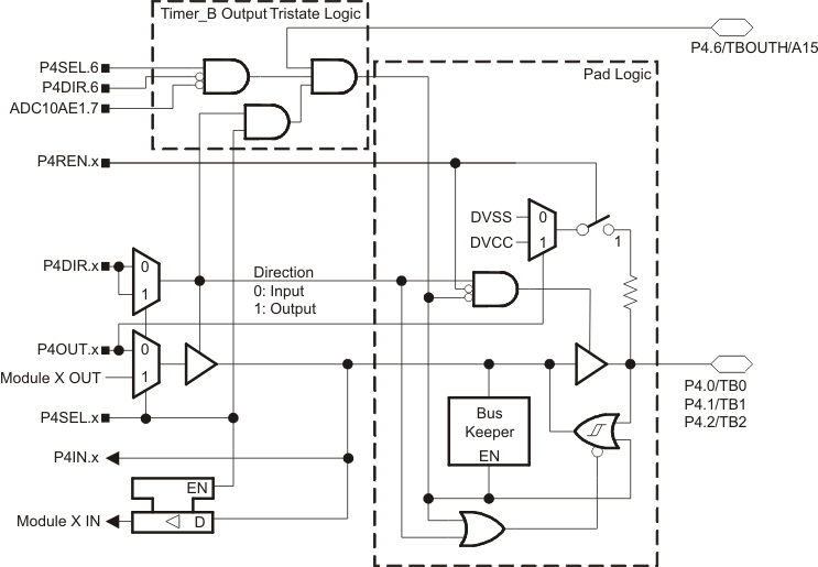
Table 6-24 Port P4 (P4.0 to P4.2) Pin Functions
| PIN NAME (P4.x) | x | FUNCTION | CONTROL BITS OR SIGNALS | |
|---|---|---|---|---|
| P4DIR.x | P4SEL.x | |||
| P4.0/TB0 | 0 | P4.0(1) (I/O) | I: 0; O: 1 | 0 |
| Timer_B3.CCI0A | 0 | 1 | ||
| Timer_B3.TB0 | 1 | 1 | ||
| P4.1/TB1 | 1 | P4.1(1) (I/O) | I: 0; O: 1 | 0 |
| Timer_B3.CCI1A | 0 | 1 | ||
| Timer_B3.TB1 | 1 | 1 | ||
| P4.2/TB2 | 2 | P4.2(1) (I/O) | I: 0; O: 1 | 0 |
| Timer_B3.CCI2A | 0 | 1 | ||
| Timer_B3.TB2 | 1 | 1 | ||
6.19.15 Port P4 Pin Schematic: P4.3 to P4.4, Input/Output With Schmitt Trigger
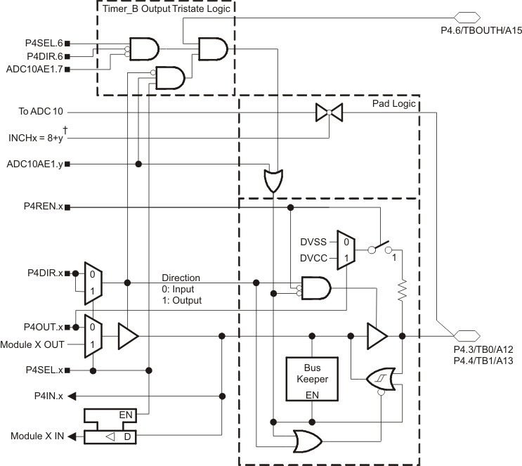
Table 6-25 Port P4 (P4.3 to P4.4) Pin Functions
| PIN NAME (P4.x) | x | y | FUNCTION | CONTROL BITS OR SIGNALS(1) | ||
|---|---|---|---|---|---|---|
| P4DIR.x | P4SEL.x | ADC10AE1.y | ||||
| P4.3/TB0/A12 | 3 | 4 | P4.3(2) (I/O) | I: 0; O: 1 | 0 | 0 |
| Timer_B3.CCI0B | 0 | 1 | 0 | |||
| Timer_B3.TB0 | 1 | 1 | 0 | |||
| A12(3) | X | X | 1 | |||
| P4.4/TB1/A13 | 4 | 5 | P4.4(2) (I/O) | I: 0; O: 1 | 0 | 0 |
| Timer_B3.CCI1B | 0 | 1 | 0 | |||
| Timer_B3.TB1 | 1 | 1 | 0 | |||
| A13(3) | X | X | 1 | |||
6.19.16 Port P4 Pin Schematic: P4.5, Input/Output With Schmitt Trigger
Table 6-26 Port P4 (P4.5) Pin Functions
| PIN NAME (P4.x) | x | y | FUNCTION | CONTROL BITS OR SIGNALS(1) | ||
|---|---|---|---|---|---|---|
| P4DIR.x | P4SEL.x | ADC10AE1.y | ||||
| P4.5/TB3/A14 | 5 | 6 | P4.5(2) (I/O) | I: 0; O: 1 | 0 | 0 |
| Timer_B3.TB2 | 1 | 1 | 0 | |||
| A14(3) | X | X | 1 | |||
6.19.17 Port P4 Pin Schematic: P4.6, Input/Output With Schmitt Trigger
Table 6-27 Port P4 (P4.6) Pin Functions
| PIN NAME (P4.x) | x | y | FUNCTION | CONTROL BITS OR SIGNALS(1) | ||
|---|---|---|---|---|---|---|
| P4DIR.x | P4SEL.x | ADC10AE1.y | ||||
| P4.6/TBOUTH/A15 | 6 | 7 | P4.6(2) (I/O) | I: 0; O: 1 | 0 | 0 |
| TBOUTH | 0 | 1 | 0 | |||
| DVSS | 1 | 1 | 0 | |||
| A15(3) | X | X | 1 | |||
6.19.18 Port P4 Pin Schematic: P4.7, Input/Output With Schmitt Trigger
Table 6-28 Port P4 (Pr.7) Pin Functions
| PIN NAME (P4.x) | x | FUNCTION | CONTROL BITS OR SIGNALS | |
|---|---|---|---|---|
| P4DIR.x | P4SEL.x | |||
| P4.7/TBCLK | 7 | P4.7(1) (I/O) | I: 0; O: 1 | 0 |
| Timer_B3.TBCLK | 0 | 1 | ||
| DVSS | 1 | 1 | ||
6.19.19 JTAG Fuse Check Mode
MSP430 devices that have the fuse on the TEST terminal have a fuse check mode that tests the continuity of the fuse the first time the JTAG port is accessed after a power-on reset (POR). When activated, a fuse check current, ITF , of 1 mA at 3 V, 2.5 mA at 5 V can flow from the TEST pin to ground if the fuse is not burned. Care must be taken to avoid accidentally activating the fuse check mode and increasing overall system power consumption.
When the TEST pin is again taken low after a test or programming session, the fuse check mode and sense currents are terminated.
Activation of the fuse check mode occurs with the first negative edge on the TMS pin after power up or if TMS is held low during power up. The second positive edge on the TMS pin deactivates the fuse check mode. After deactivation, the fuse check mode remains inactive until another POR occurs. After each POR, the fuse check mode has the potential to be activated.
The fuse check current flows only when the fuse check mode is active and the TMS pin is in a low state (see Figure 6-1). Therefore, the additional current flow can be prevented by holding the TMS pin high (default condition).
 Figure 6-1 Fuse Check Mode Current
NOTE
The CODE and RAM data protection is ensured if the JTAG fuse is blown and the 256-bit bootloader access key is used. Also, see the Bootstrap Loader section for more information.