SLAS892C March 2013 – September 2014 MSP430G2444 , MSP430G2544 , MSP430G2744
PRODUCTION DATA.
- 1Device Overview
- 2Revision History
- 3Device Comparison
- 4Terminal Configuration and Functions
-
5Specifications
- 5.1 Absolute Maximum Ratings
- 5.2 Handling Ratings
- 5.3 Recommended Operating Conditions
- 5.4 Active Mode Supply Current (Into DVCC + AVCC) Excluding External Current
- 5.5 Typical Characteristics - Active-Mode Supply Current (Into DVCC + AVCC)
- 5.6 Low-Power-Mode Supply Currents (Into VCC ) Excluding External Current
- 5.7 Schmitt-Trigger Inputs (Ports P1, P2, P3, P4, and RST/NMI)
- 5.8 Leakage Current, Ports Px
- 5.9 Outputs, Ports Px
- 5.10 Output Frequency, Ports Px
- 5.11 Typical Characteristics - Outputs
- 5.12 POR and BOR
- 5.13 Typical Characteristics - POR and BOR
- 5.14 DCO Frequency
- 5.15 Calibrated DCO Frequencies, Tolerance
- 5.16 Wake-Up From Lower-Power Modes (LPM3, LPM4)
- 5.17 Typical Characteristics - DCO Clock Wake-Up Time From LPM3 or LPM4
- 5.18 DCO With External Resistor ROSC
- 5.19 Typical Characteristics - DCO With External Resistor ROSC
- 5.20 Crystal Oscillator LFXT1, Low-Frequency Mode
- 5.21 Internal Very-Low-Power Low-Frequency Oscillator (VLO)
- 5.22 Crystal Oscillator LFXT1, High-Frequency Mode
- 5.23 Typical Characteristics - LFXT1 Oscillator in HF Mode (XTS = 1)
- 5.24 Timer_A, Timer_B
- 5.25 USCI (UART Mode)
- 5.26 USCI (SPI Master Mode)
- 5.27 USCI (SPI Slave Mode)
- 5.28 USCI (I2C Mode)
- 5.29 10-Bit ADC, Power Supply and Input Range Conditions
- 5.30 10-Bit ADC, Built-In Voltage Reference
- 5.31 10-Bit ADC, External Reference
- 5.32 10-Bit ADC, Timing Parameters
- 5.33 10-Bit ADC, Linearity Parameters
- 5.34 10-Bit ADC, Temperature Sensor and Built-In VMID
- 5.35 Flash Memory
- 5.36 RAM
- 5.37 JTAG and Spy-Bi-Wire Interface
- 5.38 JTAG Fuse
-
6Detailed Description
- 6.1 CPU
- 6.2 Instruction Set
- 6.3 Operating Modes
- 6.4 Interrupt Vector Addresses
- 6.5 Special Function Registers
- 6.6 Memory Organization
- 6.7 Bootstrap Loader (BSL)
- 6.8 Flash Memory
- 6.9 Peripherals
- 6.10 Oscillator and System Clock
- 6.11 Brownout
- 6.12 Digital I/O
- 6.13 Watchdog Timer (WDT+)
- 6.14 Timer_A3
- 6.15 Timer_B3
- 6.16 Universal Serial Communications Interface (USCI)
- 6.17 ADC10
- 6.18 Peripheral File Map
- 6.19
Port Schematics
- 6.19.1 Port P1 Pin Schematic: P1.0 to P1.3, Input/Output With Schmitt Trigger
- 6.19.2 Port P1 Pin Schematic: P1.4 to P1.6, Input/Output With Schmitt Trigger and In-System Access Features
- 6.19.3 Port P1 Pin Schematic: P1.7, Input/Output With Schmitt Trigger and In-System Access Features
- 6.19.4 Port P2 Pin Schematic: P2.0, P2.2, Input/Output With Schmitt Trigger
- 6.19.5 Port P2 Pin Schematic: P2.1, Input/Output With Schmitt Trigger
- 6.19.6 Port P2 Pin Schematic: P2.3, Input/Output With Schmitt Trigger
- 6.19.7 Port P2 Pin Schematic: P2.4, Input/Output With Schmitt Trigger
- 6.19.8 Port P2 Pin Schematic: P2.5, Input/Output With Schmitt Trigger and External ROSC for DCO
- 6.19.9 Port P2 Pin Schematic: P2.6, Input/Output With Schmitt Trigger and Crystal Oscillator Input
- 6.19.10 Port P2 Pin Schematic: P2.7, Input/Output With Schmitt Trigger and Crystal Oscillator Output
- 6.19.11 Port P3 Pin Schematic: P3.0, Input/Output With Schmitt Trigger
- 6.19.12 Port P3 Pin Schematic: P3.1 to P3.5, Input/Output With Schmitt Trigger
- 6.19.13 Port P3 Pin Schematic: P3.6 to P3.7, Input/Output With Schmitt Trigger
- 6.19.14 Port P4 Pin Schematic: P4.0 to P4.2, Input/Output With Schmitt Trigger
- 6.19.15 Port P4 Pin Schematic: P4.3 to P4.4, Input/Output With Schmitt Trigger
- 6.19.16 Port P4 Pin Schematic: P4.5, Input/Output With Schmitt Trigger
- 6.19.17 Port P4 Pin Schematic: P4.6, Input/Output With Schmitt Trigger
- 6.19.18 Port P4 Pin Schematic: P4.7, Input/Output With Schmitt Trigger
- 6.19.19 JTAG Fuse Check Mode
-
7Device and Documentation Support
- 7.1 Device Support
- 7.2 Documentation Support
- 7.3 Related Links
- 7.4 Community Resources
- 7.5 Trademarks
- 7.6 Electrostatic Discharge Caution
- 7.7 Glossary
- 8Mechanical, Packaging, and Orderable Information
Package Options
Mechanical Data (Package|Pins)
Thermal pad, mechanical data (Package|Pins)
Orderable Information
5 Specifications
5.1 Absolute Maximum Ratings(1)(2)
| MIN | MAX | UNIT | |
|---|---|---|---|
| Voltage applied at VCC | -0.3 | 4.1 | V |
| Voltage applied to any pin(3) | -0.3 | VCC + 0.3 | V |
| Diode current at any device terminal | ±2 | mA |
(1) Stresses beyond those listed under Absolute Maximum Ratings may cause permanent damage to the device. These are stress ratings only, and functional operation of the device at these or any other conditions beyond those indicated under Recommended Operating Conditions is not implied. Exposure to absolute-maximum-rated conditions for extended periods may affect device reliability.
(2) All voltages referenced to VSS.
(3) The JTAG fuse-blow voltage, VFB, is allowed to exceed the absolute maximum rating. The voltage is applied to the TEST pin when blowing the JTAG fuse.
5.2 Handling Ratings
| MIN | MAX | UNIT | ||
|---|---|---|---|---|
| Tstg | Storage temperature (programmed or unprogrammed device)(1) | -55 | 150 | °C |
(1) Higher temperature may be applied during board soldering process according to the current JEDEC J-STD-020 specification with peak reflow temperatures not higher than classified on the device label on the shipping boxes or reels.
5.3 Recommended Operating Conditions(1)(2)
Typical values are specified at VCC = 3.3 V and TA = 25°C (unless otherwise noted)| MIN | NOM | MAX | UNIT | ||||
|---|---|---|---|---|---|---|---|
| VCC | Supply voltage | AVCC = DVCC = VCC | During program execution | 1.8 | 3.6 | V | |
| During program and erase of flash memory | 2.2 | 3.6 | V | ||||
| VSS | Supply voltage | AVSS = DVSS = VSS | 0 | V | |||
| TA | Operating free-air temperature | -40 | 85 | °C | |||
| fSYSTEM | Processor frequency (maximum MCLK frequency)(1)(2) (see Figure 5-1) |
VCC = 1.8 V, Duty cycle = 50% ±10% | dc | 4.15 | MHz | ||
| VCC = 2.7 V, Duty cycle = 50% ±10% | dc | 12 | |||||
| VCC ≥ 3.3 V, Duty cycle = 50% ±10% | dc | 16 | |||||
(1) The MSP430 CPU is clocked directly with MCLK. Both the high and low phase of MCLK must not exceed the pulse width of the specified maximum frequency.
(2) Modules might have a different maximum input clock specification. See the specification of the respective module in this data sheet.
A. Minimum processor frequency is defined by system clock. Flash program or erase operations require a minimum VCC of 2.2 V.
Figure 5-1 Operating Area
5.4 Active Mode Supply Current (Into DVCC + AVCC) Excluding External Current(1)(2)
over recommended ranges of supply voltage and operating free-air temperature (unless otherwise noted)| PARAMETER | TEST CONDITIONS | TA | VCC | MIN | TYP | MAX | UNIT | |
|---|---|---|---|---|---|---|---|---|
| IAM,1MHz | Active mode (AM) current (1 MHz) | fDCO = fMCLK = fSMCLK = 1 MHz, fACLK = 32768 Hz, Program executes in flash, BCSCTL1 = CALBC1_1MHZ, DCOCTL = CALDCO_1MHZ, CPUOFF = 0, SCG0 = 0, SCG1 = 0, OSCOFF = 0 |
2.2 V | 270 | µA | |||
| 3 V | 390 | 550 | ||||||
(1) All inputs are tied to 0 V or VCC . Outputs do not source or sink any current.
(2) The currents are characterized with a Micro Crystal CC4V-T1A SMD crystal with a load capacitance of 9 pF. The internal and external load capacitance is chosen to closely match the required 9 pF.
5.5 Typical Characteristics - Active-Mode Supply Current (Into DVCC + AVCC)
| TA = 25°C |
5.6 Low-Power-Mode Supply Currents (Into VCC ) Excluding External Current(1)(2)
over recommended ranges of supply voltage and operating free-air temperature (unless otherwise noted)| PARAMETER | TEST CONDITIONS | TA | VCC | MIN | TYP | MAX | UNIT | |
|---|---|---|---|---|---|---|---|---|
| ILPM0,1MHz | Low-power mode 0 (LPM0) current(3) | fMCLK = 0 MHz, fSMCLK = fDCO = 1 MHz, fACLK = 32768 Hz, BCSCTL1 = CALBC1_1MHZ, DCOCTL = CALDCO_1MHZ, CPUOFF = 1, SCG0 = 0, SCG1 = 0, OSCOFF = 0 |
25°C | 2.2 V | 75 | 90 | µA | |
| ILPM2 | Low-power mode 2 (LPM2) current(4) | fMCLK = fSMCLK = 0 MHz, fDCO = 1 MHz, fACLK = 32768 Hz, BCSCTL1 = CALBC1_1MHZ, DCOCTL = CALDCO_1MHZ, CPUOFF = 1, SCG0 = 0, SCG1 = 1, OSCOFF = 0 |
25°C | 2.2 V | 22 | µA | ||
| ILPM3,LFXT1 | Low-power mode 3 (LPM3) current(4) | fDCO = fMCLK = fSMCLK = 0 MHz, fACLK = 32768 Hz, CPUOFF = 1, SCG0 = 1, SCG1 = 1, OSCOFF = 0 |
25°C | 2.2 V | 1 | 2 | µA | |
| ILPM3,VLO | Low-power mode 3 current, (LPM3)(4) | fDCO = fMCLK = fSMCLK = 0 MHz, fACLK from internal LF oscillator (VLO), CPUOFF = 1, SCG0 = 1, SCG1 = 1, OSCOFF = 0 |
25°C | 2.2 V | 0.5 | 1 | µA | |
| ILPM4 | Low-power mode 4 (LPM4) current(5) | fDCO = fMCLK = fSMCLK = 0 MHz, fACLK = 0 Hz, CPUOFF = 1, SCG0 = 1, SCG1 = 1, OSCOFF = 1 |
25°C | 2.2 V | 0.1 | 0.5 | µA | |
| 85°C | 1.5 | 3 | ||||||
(1) All inputs are tied to 0 V or VCC . Outputs do not source or sink any current.
(2) The currents are characterized with a Micro Crystal CC4V-T1A SMD crystal with a load capacitance of 9 pF. The internal and external load capacitance is chosen to closely match the required 9 pF.
(3) Current for brownout and WDT clocked by SMCLK included.
(4) Current for brownout and WDT clocked by ACLK included.
(5) Current for brownout included.
5.7 Schmitt-Trigger Inputs (Ports P1, P2, P3, P4, and RST/NMI)
over recommended ranges of supply voltage and operating free-air temperature (unless otherwise noted)| PARAMETER | TEST CONDITIONS | VCC | MIN | TYP | MAX | UNIT | |
|---|---|---|---|---|---|---|---|
| VIT+ | Positive-going input threshold voltage | 0.45 VCC | 0.75 VCC | V | |||
| 3 V | 1.35 | 2.25 | |||||
| VIT- | Negative-going input threshold voltage | 0.25 VCC | 0.55 VCC | V | |||
| 3 V | 0.75 | 1.65 | |||||
| Vhys | Input voltage hysteresis (VIT+ - VIT- ) | 3 V | 0.3 | 1 | V | ||
| RPull | Pullup or pulldown resistor | For pullup: VIN = VSS, For pulldown: VIN = VCC |
3 V | 20 | 35 | 50 | kΩ |
| CI | Input capacitance | VIN = VSS or VCC | 5 | pF | |||
5.8 Leakage Current, Ports Px
over recommended ranges of supply voltage and operating free-air temperature (unless otherwise noted)| PARAMETER | TEST CONDITIONS | VCC | MIN | TYP | MAX | UNIT | |
|---|---|---|---|---|---|---|---|
| Ilkg(Px.y) | High-impedance leakage current | (1)(2) | 3 V | ±50 | nA | ||
(1) The leakage current is measured with VSS or VCC applied to the corresponding pin(s), unless otherwise noted.
(2) The leakage of the digital port pins is measured individually. The port pin is selected for input and the pullup or pulldown resistor is disabled.
5.9 Outputs, Ports Px
over recommended ranges of supply voltage and operating free-air temperature (unless otherwise noted)| PARAMETER | TEST CONDITIONS | VCC | MIN | TYP | MAX | UNIT | |
|---|---|---|---|---|---|---|---|
| VOH | High-level output voltage | IOH(max) = -6 mA (1) | 3 V | VCC - 0.3 | V | ||
| VOL | Low-level output voltage | IOL(max) = 6 mA(1) | 3 V | VSS + 0.3 | V | ||
(1) The maximum total current, IOH(max) and IOL(max), for all outputs combined, should not exceed ±48 mA to hold the maximum voltage drop specified.
5.10 Output Frequency, Ports Px
over recommended ranges of supply voltage and operating free-air temperature (unless otherwise noted)| PARAMETER | TEST CONDITIONS | VCC | MIN | TYP | MAX | UNIT | |
|---|---|---|---|---|---|---|---|
| fPx.y | Port output frequency (with load) | Px.y, CL = 20 pF, RL = 1 kΩ against VCC/2(1)(2) |
3 V | 12 | MHz | ||
| fPort_CLK | Clock output frequency | Px.y, CL = 20 pF(2) | 3 V | 16 | MHz | ||
(1) Alternatively, a resistive divider with two 2-kΩ resistors between VCC and VSS is used as load. The output is connected to the center tap of the divider.
(2) The output voltage reaches at least 10% and 90% VCC at the specified toggle frequency.
5.11 Typical Characteristics - Outputs
One output loaded at a time.
 Figure 5-4 Typical Low-Level Output Current vs Low-Level Output Voltage
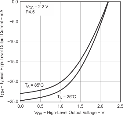 Figure 5-6 Typical High-Level Output Current vs High-Level Output Voltage
 Figure 5-5 Typical Low-Level Output Current vs Low-Level Output Voltage
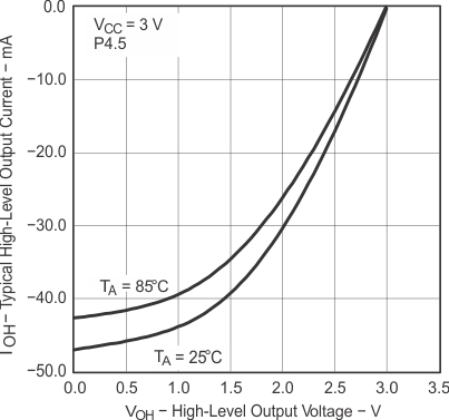 Figure 5-7 Typical High-Level Output Current vs High-Level Output Voltage
5.12 POR and BOR(1)(2)
over recommended ranges of supply voltage and operating free-air temperature (unless otherwise noted)| PARAMETER | TEST CONDITIONS | VCC | MIN | TYP | MAX | UNIT | |
|---|---|---|---|---|---|---|---|
| VCC(start) | See Figure 5-8 | dVCC /dt ≤ 3 V/s | 0.7 × V(B_IT-) | V | |||
| V(B_IT-) | See Figure 5-8 through Figure 5-10 | dVCC /dt ≤ 3 V/s | 1.35 | V | |||
| Vhys(B_IT-) | See Figure 5-8 | dVCC /dt ≤ 3 V/s | 140 | mV | |||
| td(BOR) | See Figure 5-8 | 2000 | µs | ||||
| t(reset) | Pulse duration needed at RST/NMI pin to accept reset internally | 2.2 V | 2 | µs | |||
(1) The current consumption of the brownout module is already included in the ICC current consumption data. The voltage level V(B_IT-) + Vhys(B_IT-) is ≤ 1.8 V.
(2) During power up, the CPU begins code execution following a period of td(BOR) after VCC = V(B_IT-) + Vhys(B_IT-) . The default DCO settings must not be changed until VCC ≥ VCC(min), where VCC(min) is the minimum supply voltage for the desired operating frequency.
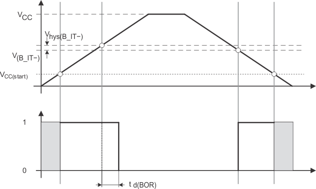 Figure 5-8 POR and BOR vs Supply Voltage
5.13 Typical Characteristics - POR and BOR
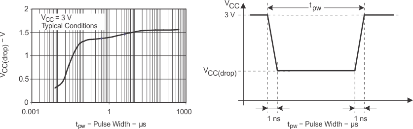 Figure 5-9 VCC(drop) Level With a Square Voltage Drop to Generate a POR or BOR Signal
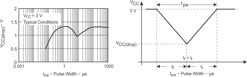 Figure 5-10 VCC(drop) Level With a Triangular Voltage Drop to Generate a POR or BOR Signal
5.14 DCO Frequency
over recommended ranges of supply voltage and operating free-air temperature (unless otherwise noted)| PARAMETER | TEST CONDITIONS | VCC | MIN | TYP | MAX | UNIT | |
|---|---|---|---|---|---|---|---|
| VCC | Supply voltage range | RSELx < 14 | 1.8 | 3.6 | V | ||
| RSELx = 14 | 2.2 | 3.6 | |||||
| RSELx = 15 | 3.0 | 3.6 | |||||
| fDCO(0,0) | DCO frequency (0, 0) | RSELx = 0, DCOx = 0, MODx = 0 | 3 V | 0.06 | 0.14 | MHz | |
| fDCO(0,3) | DCO frequency (0, 3) | RSELx = 0, DCOx = 3, MODx = 0 | 3 V | 0.07 | 0.17 | MHz | |
| fDCO(1,3) | DCO frequency (1, 3) | RSELx = 1, DCOx = 3, MODx = 0 | 3 V | MHz | |||
| fDCO(2,3) | DCO frequency (2, 3) | RSELx = 2, DCOx = 3, MODx = 0 | 3 V | MHz | |||
| fDCO(3,3) | DCO frequency (3, 3) | RSELx = 3, DCOx = 3, MODx = 0 | 3 V | MHz | |||
| fDCO(4,3) | DCO frequency (4, 3) | RSELx = 4, DCOx = 3, MODx = 0 | 3 V | MHz | |||
| fDCO(5,3) | DCO frequency (5, 3) | RSELx = 5, DCOx = 3, MODx = 0 | 3 V | MHz | |||
| fDCO(6,3) | DCO frequency (6, 3) | RSELx = 6, DCOx = 3, MODx = 0 | 3 V | 0.54 | 1.06 | MHz | |
| fDCO(7,3) | DCO frequency (7, 3) | RSELx = 7, DCOx = 3, MODx = 0 | 3 V | 0.80 | 1.50 | MHz | |
| fDCO(8,3) | DCO frequency (8, 3) | RSELx = 8, DCOx = 3, MODx = 0 | 3 V | 1.6 | MHz | ||
| fDCO(9,3) | DCO frequency (9, 3) | RSELx = 9, DCOx = 3, MODx = 0 | 3 V | 2.3 | MHz | ||
| fDCO(10,3) | DCO frequency (10, 3) | RSELx = 10, DCOx = 3, MODx = 0 | 3 V | 3.4 | MHz | ||
| fDCO(11,3) | DCO frequency (11, 3) | RSELx = 11, DCOx = 3, MODx = 0 | 3 V | 4.25 | MHz | ||
| fDCO(12,3) | DCO frequency (12, 3) | RSELx = 12, DCOx = 3, MODx = 0 | 3 V | 4.30 | 7.30 | MHz | |
| fDCO(13,3) | DCO frequency (13, 3) | RSELx = 13, DCOx = 3, MODx = 0 | 3 V | 6.00 | 9.60 | MHz | |
| fDCO(14,3) | DCO frequency (14, 3) | RSELx = 14, DCOx = 3, MODx = 0 | 3 V | 8.60 | 13.9 | MHz | |
| fDCO(15,3) | DCO frequency (15, 3) | RSELx = 15, DCOx = 3, MODx = 0 | 3 V | 12.0 | 18.5 | MHz | |
| fDCO(15,7) | DCO frequency (15, 7) | RSELx = 15, DCOx = 7, MODx = 0 | 3 V | 16.0 | 26.0 | MHz | |
| SRSEL | Frequency step between range RSEL and RSEL+1 | SRSEL = fDCO(RSEL+1,DCO) /fDCO(RSEL,DCO) | 3 V | 1.35 | ratio | ||
| SDCO | Frequency step between tap DCO and DCO+1 | SDCO = fDCO(RSEL,DCO+1) /fDCO(RSEL,DCO) | 3 V | 1.08 | ratio | ||
| Duty cycle | Measured at SMCLK | 3 V | 50% | ||||
5.15 Calibrated DCO Frequencies, Tolerance
over recommended ranges of supply voltage and operating free-air temperature (unless otherwise noted)| PARAMETER | TEST CONDITIONS | TA | VCC | MIN | TYP | MAX | UNIT |
|---|---|---|---|---|---|---|---|
| 1-MHz tolerance over temperature(1) | BCSCTL1 = CALBC1_1MHZ, DCOCTL = CALDCO_1MHZ, calibrated at 30°C and 3 V |
0°C to 85°C | 3 V | -3% | ±0.5% | +3% | |
| 1-MHz tolerance over VCC | BCSCTL1 = CALBC1_1MHZ, DCOCTL = CALDCO_1MHZ, calibrated at 30°C and 3 V |
30°C | 1.8 V to 3.6 V | -3% | ±2% | +3% | |
| 1-MHz tolerance overall | BCSCTL1 = CALBC1_1MHZ, DCOCTL = CALDCO_1MHZ, calibrated at 30°C and 3 V |
-40°C to 85°C | 1.8 V to 3.6 V | -6% | ±3% | +6% | |
| 8-MHz tolerance over temperature(1) | BCSCTL1 = CALBC1_8MHZ, DCOCTL = CALDCO_8MHZ, calibrated at 30°C and 3 V |
0°C to 85°C | 3 V | -3% | ±0.5% | +3% | |
| 8-MHz tolerance over VCC | BCSCTL1 = CALBC1_8MHZ, DCOCTL = CALDCO_8MHZ, calibrated at 30°C and 3 V |
30°C | 2.2 V to 3.6 V | -3% | ±2% | +3% | |
| 8-MHz tolerance overall | BCSCTL1 = CALBC1_8MHZ, DCOCTL = CALDCO_8MHZ, calibrated at 30°C and 3 V |
-40°C to 85°C | 2.2 V to 3.6 V | -6% | ±3% | +6% | |
| 12-MHz tolerance over temperature(1) | BCSCTL1 = CALBC1_12MHZ, DCOCTL = CALDCO_12MHZ, calibrated at 30°C and 3 V |
0°C to 85°C | 3 V | -3% | ±0.5% | +3% | |
| 12-MHz tolerance over VCC | BCSCTL1 = CALBC1_12MHZ, DCOCTL = CALDCO_12MHZ, calibrated at 30°C and 3 V |
30°C | 2.7 V to 3.6 V | -3% | ±2% | +3% | |
| 12-MHz tolerance overall | BCSCTL1 = CALBC1_12MHZ, DCOCTL = CALDCO_12MHZ, calibrated at 30°C and 3 V |
-40°C to 85°C | 2.7 V to 3.6 V | -6% | ±3% | +6% | |
| 16-MHz tolerance over temperature(1) | BCSCTL1 = CALBC1_16MHZ, DCOCTL = CALDCO_16MHZ, calibrated at 30°C and 3 V |
0°C to 85°C | 3 V | -3% | ±0.5% | +3% | |
| 16-MHz tolerance over VCC | BCSCTL1 = CALBC1_16MHZ, DCOCTL = CALDCO_16MHZ, calibrated at 30°C and 3 V |
30°C | 3.3 V to 3.6 V | -3% | ±2% | +3% | |
| 16-MHz tolerance overall | BCSCTL1 = CALBC1_16MHZ, DCOCTL = CALDCO_16MHZ, calibrated at 30°C and 3 V |
-40°C to 85°C | 3.3 V to 3.6 V | -6% | ±3% | +6% |
(1) This is the frequency change from the measured frequency at 30°C over temperature.
5.16 Wake-Up From Lower-Power Modes (LPM3, LPM4)
over recommended ranges of supply voltage and operating free-air temperature (unless otherwise noted)| PARAMETER | TEST CONDITIONS | VCC | MIN | TYP | MAX | UNIT | |
|---|---|---|---|---|---|---|---|
| tDCO,LPM3/4 | DCO clock wake-up time from LPM3 or LPM4 (1) | BCSCTL1 = CALBC1_1MHZ, DCOCTL = CALDCO_1MHZ | 3 V | 1.5 | µs | ||
| tCPU,LPM3/4 | CPU wake-up time from LPM3 or LPM4 (2) | 1 / fMCLK + tClock,LPM3/4 |
|||||
(1) The DCO clock wake-up time is measured from the edge of an external wake-up signal (for example, a port interrupt) to the first clock edge observable externally on a clock pin (MCLK or SMCLK).
(2) Parameter applicable only if DCOCLK is used for MCLK.
5.17 Typical Characteristics - DCO Clock Wake-Up Time From LPM3 or LPM4
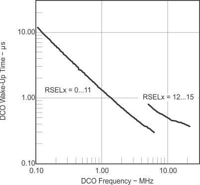 Figure 5-11 Clock Wake-Up Time From LPM3 vs DCO Frequency
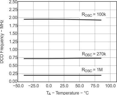
5.18 DCO With External Resistor ROSC(1)
over recommended ranges of supply voltage and operating free-air temperature (unless otherwise noted)| PARAMETER | TEST CONDITIONS | VCC | MIN | TYP | MAX | UNIT | |
|---|---|---|---|---|---|---|---|
| fDCO,ROSC | DCO output frequency with ROSC | DCOR = 1, RSELx = 4, DCOx = 3, MODx = 0, TA = 25°C |
2.2 V | 1.8 | MHz | ||
| 3 V | 1.95 | ||||||
| DT | Temperature drift | DCOR = 1, RSELx = 4, DCOx = 3, MODx = 0 |
2.2 V, 3 V | ±0.1 | %/°C | ||
| DV | Drift with VCC | DCOR = 1, RSELx = 4, DCOx = 3, MODx = 0 |
2.2 V, 3 V | 10 | %/V | ||
(1) ROSC = 100 kΩ. Metal film resistor, type 0257, 0.6 W with 1% tolerance and TK = ±50 ppm/°C.
5.19 Typical Characteristics - DCO With External Resistor ROSC

| VCC = 2.2 V | TA = 25°C |
| VCC = 3 V |
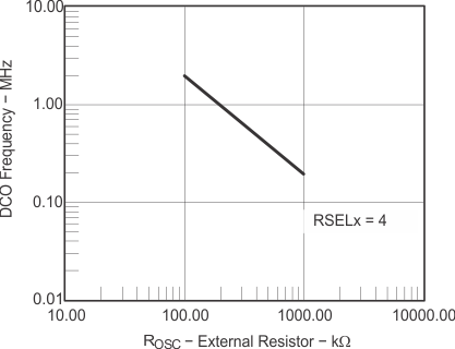
| VCC = 3 V | TA = 25°C |
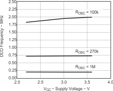
| TA = 25°C |
5.20 Crystal Oscillator LFXT1, Low-Frequency Mode(4)
over recommended ranges of supply voltage and operating free-air temperature (unless otherwise noted)| PARAMETER | TEST CONDITIONS | VCC | MIN | TYP | MAX | UNIT | |
|---|---|---|---|---|---|---|---|
| fLFXT1,LF | LFXT1 oscillator crystal frequency, LF mode 0, 1 | XTS = 0, LFXT1Sx = 0 or 1 | 1.8 V to 3.6 V | 32768 | Hz | ||
| fLFXT1,LF,logic | LFXT1 oscillator logic level square wave input frequency, LF mode | XTS = 0, XCAPx = 0, LFXT1Sx = 3 | 1.8 V to 3.6 V | 10000 | 32768 | 50000 | Hz |
| OALF | Oscillation allowance for LF crystals | XTS = 0, LFXT1Sx = 0, fLFXT1,LF = 32768 Hz, CL,eff = 6 pF |
500 | kΩ | |||
| XTS = 0, LFXT1Sx = 0, fLFXT1,LF = 32768 Hz, CL,eff = 12 pF |
200 | ||||||
| CL,eff | Integrated effective load capacitance, LF mode(1) | XTS = 0, XCAPx = 0 | 1 | pF | |||
| XTS = 0, XCAPx = 1 | 5.5 | ||||||
| XTS = 0, XCAPx = 2 | 8.5 | ||||||
| XTS = 0, XCAPx = 3 | 11 | ||||||
| Duty cycle, LF mode | XTS = 0, Measured at P2.0/ACLK, fLFXT1,LF = 32768 Hz |
2.2 V | 30% | 50% | 70% | ||
| fFault,LF | Oscillator fault frequency, LF mode(3) | XTS = 0, XCAPx = 0, LFXT1Sx = 3(2) | 2.2 V | 10 | 10000 | Hz | |
(1) Includes parasitic bond and package capacitance (approximately 2 pF per pin).
Because the PCB adds additional capacitance, it is recommended to verify the correct load by measuring the ACLK frequency. For a correct setup, the effective load capacitance should always match the specification of the crystal that is used.
Because the PCB adds additional capacitance, it is recommended to verify the correct load by measuring the ACLK frequency. For a correct setup, the effective load capacitance should always match the specification of the crystal that is used.
(2) Measured with logic-level input frequency but also applies to operation with crystals.
(3) Frequencies below the MIN specification set the fault flag. Frequencies above the MAX specification do not set the fault flag. Frequencies between the MIN and MAX specifications might set the flag.
(4) To improve EMI on the XT1 oscillator, the following guidelines should be observed.
- Keep the trace between the device and the crystal as short as possible.
- Design a good ground plane around the oscillator pins.
- Prevent crosstalk from other clock or data lines into oscillator pins XIN and XOUT.
- Avoid running PCB traces underneath or adjacent to the XIN and XOUT pins.
- Use assembly materials and processes that avoid any parasitic load on the oscillator XIN and XOUT pins.
- If conformal coating is used, make sure that it does not induce capacitive or resistive leakage between the oscillator pins.
- Do not route the XOUT line to the JTAG header to support the serial programming adapter as shown in other documentation. This signal is no longer required for the serial programming adapter.
5.21 Internal Very-Low-Power Low-Frequency Oscillator (VLO)
over recommended ranges of supply voltage and operating free-air temperature (unless otherwise noted)| PARAMETER | TA | VCC | MIN | TYP | MAX | UNIT | |
|---|---|---|---|---|---|---|---|
| fVLO | VLO frequency | -40°C to 85°C | 3 V | 4 | 12 | 20 | kHz |
| dfVLO/dT | VLO frequency temperature drift (1) | -40°C to 85°C | 3 V | 0.5 | %/°C | ||
| dfVLO/dVCC | VLO frequency supply voltage drift (2) | 25°C | 1.8 V to 3.6 V | 4 | %/V | ||
(1) Calculated using the box method:
I version: [MAX(-40...85°C) - MIN(-40...85°C)]/MIN(-40...85°C)/[85°C - (-40°C)]
I version: [MAX(-40...85°C) - MIN(-40...85°C)]/MIN(-40...85°C)/[85°C - (-40°C)]
(2) Calculated using the box method: [MAX(1.8...3.6 V) - MIN(1.8...3.6 V)]/MIN(1.8...3.6 V)/(3.6 V - 1.8 V)
5.22 Crystal Oscillator LFXT1, High-Frequency Mode(5)
| PARAMETER | TEST CONDITIONS | VCC | MIN | TYP | MAX | UNIT | |
|---|---|---|---|---|---|---|---|
| fLFXT1,HF0 | LFXT1 oscillator crystal frequency, HF mode 0 | XTS = 1, LFXT1Sx = 0 | 1.8 V to 3.6 V | 0.4 | 1 | MHz | |
| fLFXT1,HF1 | LFXT1 oscillator crystal frequency, HF mode 1 | XTS = 1, LFXT1Sx = 1 | 1.8 V to 3.6 V | 1 | 4 | MHz | |
| fLFXT1,HF2 | LFXT1 oscillator crystal frequency, HF mode 2 | XTS = 1, LFXT1Sx = 2 | 1.8 V to 3.6 V | 2 | 10 | MHz | |
| 2.2 V to 3.6 V | 2 | 12 | |||||
| 3 V to 3.6 V | 2 | 16 | |||||
| fLFXT1,HF,logic | LFXT1 oscillator logic-level square-wave input frequency, HF mode | XTS = 1, LFXT1Sx = 3 | 1.8 V to 3.6 V | 0.4 | 10 | MHz | |
| 2.2 V to 3.6 V | 0.4 | 12 | |||||
| 3 V to 3.6 V | 0.4 | 16 | |||||
| OAHF | Oscillation allowance for HF crystals (see Figure 5-16 and Figure 5-17) | XTS = 1, LFXT1Sx = 0, fLFXT1,HF = 1 MHz, CL,eff = 15 pF |
2700 | Ω | |||
| XTS = 1, LFXT1Sx = 1, fLFXT1,HF = 4 MHz, CL,eff = 15 pF |
800 | ||||||
| XTS = 1, LFXT1Sx = 2, fLFXT1,HF = 16 MHz, CL,eff = 15 pF |
300 | ||||||
| CL,eff | Integrated effective load capacitance, HF mode(1) | XTS = 1(2) | 1 | pF | |||
| Duty cycle, HF mode | XTS = 1, Measured at P2.0/ACLK, fLFXT1,HF = 10 MHz |
2.2 V | 40% | 50% | 60% | ||
| XTS = 1, Measured at P2.0/ACLK, fLFXT1,HF = 16 MHz |
40% | 50% | 60% | ||||
| fFault,HF | Oscillator fault frequency(4) | XTS = 1, LFXT1Sx = 3(3) | 2.2 V | 30 | 300 | kHz | |
(1) Includes parasitic bond and package capacitance (approximately 2 pF per pin). Because the PCB adds additional capacitance, it is recommended to verify the correct load by measuring the ACLK frequency. For a correct setup, the effective load capacitance should always match the specification of the used crystal.
(2) Requires external capacitors at both terminals. Values are specified by crystal manufacturers.
(3) Measured with logic-level input frequency, but also applies to operation with crystals.
(4) Frequencies below the MIN specification set the fault flag. Frequencies above the MAX specification do not set the fault flag. Frequencies between the MIN and MAX specifications might set the flag.
(5) To improve EMI on the XT1 oscillator the following guidelines should be observed:
- Keep the trace between the device and the crystal as short as possible.
- Design a good ground plane around the oscillator pins.
- Prevent crosstalk from other clock or data lines into oscillator pins XIN and XOUT.
- Avoid running PCB traces underneath or adjacent to the XIN and XOUT pins.
- Use assembly materials and processes that avoid any parasitic load on the oscillator XIN and XOUT pins.
- If conformal coating is used, make sure that it does not induce capacitive or resistive leakage between the oscillator pins.
- Do not route the XOUT line to the JTAG header to support the serial programming adapter as shown in other documentation. This signal is no longer required for the serial programming adapter.
5.23 Typical Characteristics - LFXT1 Oscillator in HF Mode (XTS = 1)
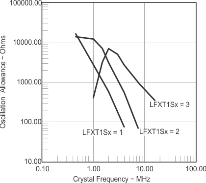
| CL,eff = 15 pF | TA = 25°C |
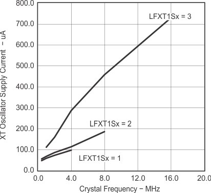
| CL,eff = 15 pF | TA = 25°C |
5.24 Timer_A, Timer_B
over recommended ranges of supply voltage and operating free-air temperature (unless otherwise noted)| PARAMETER | TEST CONDITIONS | VCC | MIN | TYP | MAX | UNIT | |
|---|---|---|---|---|---|---|---|
| fTA | Timer_A clock frequency | SMCLK, Duty cycle = 50% ± 10% | fSYSTEM | MHz | |||
| tTA,cap | Timer_A capture timing | TAx, TBx | 3 V | 20 | ns | ||
5.25 USCI (UART Mode)
over recommended ranges of supply voltage and operating free-air temperature (unless otherwise noted)| PARAMETER | TEST CONDITIONS | VCC | MIN | TYP | MAX | UNIT | |
|---|---|---|---|---|---|---|---|
| fUSCI | USCI input clock frequency | Internal: SMCLK, ACLK External: UCLK Duty cycle = 50% ± 10% |
fSYSTEM | MHz | |||
| fmax,BITCLK | Maximum BITCLK clock frequency (equals baud rate in MBaud) |
3 V | 2 | MHz | |||
| tτ | UART receive deglitch time(1) | 3 V | 50 | 100 | 600 | ns | |
(1) The DCO wake-up time must be considered in LPM3/4 for baud rates above 1 MHz.
5.26 USCI (SPI Master Mode)(1)
over recommended ranges of supply voltage and operating free-air temperature (unless otherwise noted)(see Figure 5-18 and Figure 5-19)
| PARAMETER | TEST CONDITIONS | VCC | MIN | TYP | MAX | UNIT | |
|---|---|---|---|---|---|---|---|
| fUSCI | USCI input clock frequency | SMCLK, duty cycle = 50% ± 10% | fSYSTEM | MHz | |||
| tSU,MI | SOMI input data setup time | 3 V | 75 | ns | |||
| tHD,MI | SOMI input data hold time | 3 V | 0 | ns | |||
| tVALID,MO | SIMO output data valid time | UCLK edge to SIMO valid,CL = 20 pF | 3 V | 20 | ns | ||
(1) fUCxCLK = 1/2tLO/HI with tLO/HI ≥ max(tVALID,MO(USCI) + tSU,SI(Slave), tSU,MI(USCI) + tVALID,SO(Slave)).
For the slave parameters tSU,SI(Slave) and tVALID,SO(Slave), see the SPI parameters of the attached slave.
For the slave parameters tSU,SI(Slave) and tVALID,SO(Slave), see the SPI parameters of the attached slave.
 Figure 5-18 SPI Master Mode, CKPH = 0
 Figure 5-19 SPI Master Mode, CKPH = 1
5.27 USCI (SPI Slave Mode)(1)
over recommended ranges of supply voltage and operating free-air temperature (unless otherwise noted)(see Figure 5-20 and Figure 5-21)
| PARAMETER | TEST CONDITIONS | VCC | MIN | TYP | MAX | UNIT | |
|---|---|---|---|---|---|---|---|
| tSTE,LEAD | STE lead time, STE low to clock | 3 V | 50 | ns | |||
| tSTE,LAG | STE lag time, Last clock to STE high | 3 V | 10 | ns | |||
| tSTE,ACC | STE access time, STE low to SOMI data out | 3 V | 50 | ns | |||
| tSTE,DIS | STE disable time, STE high to SOMI high impedance | 3 V | 50 | ns | |||
| tSU,SI | SIMO input data setup time | 3 V | 15 | ns | |||
| tHD,SI | SIMO input data hold time | 3 V | 10 | ns | |||
| tVALID,SO | SOMI output data valid time | UCLK edge to SOMI valid, CL = 20 pF |
3 V | 50 | 75 | ns | |
(1) fUCxCLK = 1/2tLO/HI with tLO/HI ≥ max(tVALID,MO(Master) + tSU,SI(USCI), tSU,MI(Master) + tVALID,SO(USCI)).
For the master's parameters tSU,MI(Master) and tVALID,MO(Master) refer to the SPI parameters of the attached slave.
For the master's parameters tSU,MI(Master) and tVALID,MO(Master) refer to the SPI parameters of the attached slave.
 Figure 5-20 SPI Slave Mode, CKPH = 0
 Figure 5-21 SPI Slave Mode, CKPH = 1
5.28 USCI (I2C Mode)
over recommended ranges of supply voltage and operating free-air temperature (unless otherwise noted) (see Figure 5-22)| PARAMETER | TEST CONDITIONS | VCC | MIN | TYP | MAX | UNIT | |
|---|---|---|---|---|---|---|---|
| fUSCI | USCI input clock frequency | Internal: SMCLK, ACLK External: UCLK Duty cycle = 50% ± 10% |
fSYSTEM | MHz | |||
| fSCL | SCL clock frequency | 3 V | 0 | 400 | kHz | ||
| tHD,STA | Hold time (repeated) START | fSCL ≤ 100 kHz | 3 V | 4 | µs | ||
| fSCL > 100 kHz | 0.6 | ||||||
| tSU,STA | Setup time for a repeated START | fSCL ≤ 100 kHz | 3 V | 4.7 | µs | ||
| fSCL > 100 kHz | 0.6 | ||||||
| tHD,DAT | Data hold time | 3 V | 0 | ns | |||
| tSU,DAT | Data setup time | 3 V | 250 | ns | |||
| tSU,STO | Setup time for STOP | 3 V | 4 | µs | |||
| tSP | Pulse duration of spikes suppressed by input filter | 3 V | 50 | 100 | 600 | ns | |
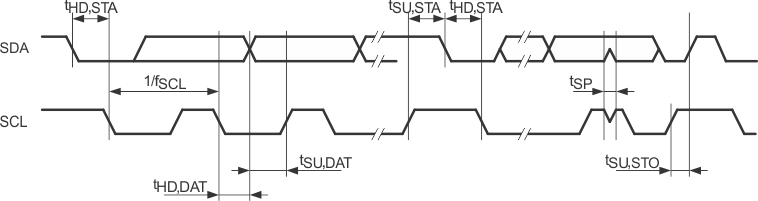 Figure 5-22 I2C Mode Timing
5.29 10-Bit ADC, Power Supply and Input Range Conditions(1)
over recommended ranges of supply voltage and operating free-air temperature (unless otherwise noted)(1)| PARAMETER | TEST CONDITIONS | TA | VCC | MIN | TYP | MAX | UNIT | |
|---|---|---|---|---|---|---|---|---|
| VCC | Analog supply voltage range | VSS = 0 V | 2.2 | 3.6 | V | |||
| VAx | Analog input voltage range(2) | All Ax terminals, Analog inputs selected in ADC10AE register |
3 V | 0 | VCC | V | ||
| IADC10 | ADC10 supply current(3) | fADC10CLK = 5 MHz, ADC10ON = 1, REFON = 0, ADC10SHT0 = 1, ADC10SHT1 = 0, ADC10DIV = 0 |
25°C | 3 V | 0.6 | mA | ||
| IREF+ | Reference supply current, reference buffer disabled(4) | fADC10CLK = 5 MHz, ADC10ON = 0, REF2_5V = 0, REFON = 1, REFOUT = 0 |
25°C | 3 V | 0.25 | mA | ||
| fADC10CLK = 5 MHz, ADC10ON = 0, REF2_5V = 1, REFON = 1, REFOUT = 0 |
0.25 | |||||||
| IREFB,0 | Reference buffer supply current with ADC10SR = 0(4) |
fADC10CLK = 5 MHz ADC10ON = 0, REFON = 1, REF2_5V = 0, REFOUT = 1, ADC10SR = 0 |
25°C | 3 V | 1.1 | mA | ||
| IREFB,1 | Reference buffer supply current with ADC10SR = 1(4) |
fADC10CLK = 5 MHz, ADC10ON = 0, REFON = 1, REF2_5V = 0, REFOUT = 1, ADC10SR = 1 |
25°C | 3 V | 0.5 | mA | ||
| CI | Input capacitance | Only one terminal Ax selected at a time | 25°C | 3 V | 27 | pF | ||
| RI | Input MUX ON resistance | 0 V ≤ VAx ≤ VCC | 25°C | 3 V | 1000 | Ω | ||
(1) The leakage current is defined in the leakage current table with Px.x/Ax parameter.
(2) The analog input voltage range must be within the selected reference voltage range VR+ to VR- for valid conversion results.
(3) The internal reference supply current is not included in current consumption parameter IADC10.
(4) The internal reference current is supplied from terminal AVCC. Consumption is independent of the ADC10ON control bit, unless a conversion is active. The REFON bit enables the built-in reference to settle before starting an A/D conversion.
5.30 10-Bit ADC, Built-In Voltage Reference
over recommended ranges of supply voltage and operating free-air temperature (unless otherwise noted)| PARAMETER | TEST CONDITIONS | VCC | MIN | TYP | MAX | UNIT | ||
|---|---|---|---|---|---|---|---|---|
| VCC,REF+ | Positive built-in reference analog supply voltage range | IVREF+ ≤ 1 mA, REF2_5V = 0 | 2.2 | V | ||||
| IVREF+ ≤ 1 mA, REF2_5V = 1 | 2.9 | |||||||
| VREF+ | Positive built-in reference voltage | IVREF+ ≤ IVREF+max, REF2_5V = 0 | 3 V | 1.41 | 1.5 | 1.59 | V | |
| IVREF+ ≤ IVREF+max, REF2_5V = 1 | 3 V | 2.35 | 2.5 | 2.65 | ||||
| ILD,VREF+ | Maximum VREF+ load current | 3 V | ±1 | mA | ||||
| VREF+ load regulation | IVREF+ = 500 µA ± 100 µA, Analog input voltage VAx ≈ 0.75 V, REF2_5V = 0 |
3 V | ±2 | LSB | ||||
| IVREF+ = 500 µA ± 100 µA, Analog input voltage VAx ≈ 1.25 V, REF2_5V = 1 |
3 V | ±2 | ||||||
| VREF+ load regulation response time | IVREF+ = 100 µA to 900 µA, VAx ≈ 0.5 x VREF+, Error of conversion result ≤1 LSB, ADC10SR = 0 |
3 V | 400 | ns | ||||
| CVREF+ | Maximum capacitance at pin VREF+ | IVREF+ ≤ ±1 mA, REFON = 1, REFOUT = 1 |
3 V | 100 | pF | |||
| TCREF+ | Temperature coefficient(1) | IVREF+ = constant with 0 mA ≤ IVREF+ ≤ 1 mA |
3 V | ±100 | ppm/°C | |||
| tREFON | Settling time of internal reference voltage | IVREF+ = 0.5 mA, REF2_5V = 0, REFON = 0 to 1 |
3.6 V | 30 | µs | |||
| tREFBURST | Settling time of reference buffer to 99.9% VREF | IVREF+ = 0.5 mA, REF2_5V = 1, REFON = 1, REFBURST = 1, ADC10SR = 0 |
3 V | 2 | µs | |||
(1) Calculated using the box method:
I temperature: (MAX(-40 to 85°C) – MIN(-40 to 85°C)) / MIN(-40 to 85°C) / (85°C – (–40°C))
I temperature: (MAX(-40 to 85°C) – MIN(-40 to 85°C)) / MIN(-40 to 85°C) / (85°C – (–40°C))
5.31 10-Bit ADC, External Reference(1)
over recommended ranges of supply voltage and operating free-air temperature (unless otherwise noted)| PARAMETER | TEST CONDITIONS | VCC | MIN | TYP | MAX | UNIT | |
|---|---|---|---|---|---|---|---|
| VeREF+ | Positive external reference input voltage range(2) | VeREF+ > VeREF-, SREF1 = 1, SREF0 = 0 |
1.4 | VCC | V | ||
| VeREF- ≤ VeREF+ ≤ VCC - 0.15 V, SREF1 = 1, SREF0 = 1(3) |
1.4 | 3 | |||||
| VeREF- | Negative external reference input voltage range(4) | VeREF+ > VeREF- | 0 | 1.2 | V | ||
| ΔVeREF | Differential external reference input voltage range ΔVeREF = VeREF+ - VeREF- |
VeREF+ > VeREF-(5) | 1.4 | VCC | V | ||
| IVeREF+ | Static input current into VeREF+ | 0 V ≤ VeREF+ ≤ VCC, SREF1 = 1, SREF0 = 0 |
3 V | ±1 | µA | ||
| 0 V ≤ VeREF+ ≤ VCC - 0.15 V ≤ 3 V, SREF1 = 1, SREF0 = 1(3) |
3 V | 0 | |||||
| IVeREF- | Static input current into VeREF- | 0 V ≤ VeREF- ≤ VCC | 3 V | ±1 | µA | ||
(1) The external reference is used during conversion to charge and discharge the capacitance array. The input capacitance, CI, is also the dynamic load for an external reference during conversion. The dynamic impedance of the reference supply should follow the recommendations on analog-source impedance to allow the charge to settle for 10-bit accuracy.
(2) The accuracy limits the minimum positive external reference voltage. Lower reference voltage levels may be applied with reduced accuracy requirements.
(3) Under this condition, the external reference is internally buffered. The reference buffer is active and requires the reference buffer supply current IREFB. The current consumption can be limited to the sample and conversion period with REBURST = 1.
(4) The accuracy limits the maximum negative external reference voltage. Higher reference voltage levels may be applied with reduced accuracy requirements.
(5) The accuracy limits the minimum external differential reference voltage. Lower differential reference voltage levels may be applied with reduced accuracy requirements.
5.32 10-Bit ADC, Timing Parameters
over recommended ranges of supply voltage and operating free-air temperature (unless otherwise noted)| PARAMETER | TEST CONDITIONS | VCC | MIN | TYP | MAX | UNIT | ||
|---|---|---|---|---|---|---|---|---|
| fADC10CLK | ADC10 input clock frequency | For specified performance of ADC10 linearity parameters | ADC10SR = 0 | 2.2 V, 3 V | 0.45 | 6.3 | MHz | |
| ADC10SR = 1 | 0.45 | 1.5 | ||||||
| fADC10OSC | ADC10 built-in oscillator frequency | ADC10DIVx = 0, ADC10SSELx = 0, fADC10CLK = fADC10OSC |
2.2 V, 3 V | 3.7 | 6.3 | MHz | ||
| tCONVERT | Conversion time | ADC10 built-in oscillator, ADC10SSELx = 0, fADC10CLK = fADC10OSC | 2.2 V, 3 V | 2.06 | 3.51 | µs | ||
| fADC10CLK from ACLK, MCLK or SMCLK, ADC10SSELx ≠ 0 | 13 × ADC10DIVx × 1 / fADC10CLK |
|||||||
| tADC10ON | Turn on settling time of the ADC(1) | 100 | ns | |||||
(1) The condition is that the error in a conversion started after tADC10ON is less than ±0.5 LSB. The reference and input signal are already settled.
5.33 10-Bit ADC, Linearity Parameters(1)
over recommended ranges of supply voltage and operating free-air temperature (unless otherwise noted)| PARAMETER | TEST CONDITIONS | VCC | MIN | TYP | MAX | UNIT | |
|---|---|---|---|---|---|---|---|
| EI | Integral linearity error | SREFx = 010 | 3 V | ±1 | LSB | ||
| ED | Differential linearity error | SREFx = 010 | 3 V | ±1 | LSB | ||
| EO | Offset error | Source impedance RS < 100 Ω, SREFx = 010 | 3 V | ±1 | LSB | ||
| EG | Gain error | SREFx = 010 | 3 V | ±1.1 | ±2 | LSB | |
| ET | Total unadjusted error | SREFx = 010 | 3 V | ±2 | ±6 | LSB | |
(1) Using the integrated reference buffer (SREFx = 010) increases the gain, and offset and total unadjusted error.
5.34 10-Bit ADC, Temperature Sensor and Built-In VMID(1)
over recommended ranges of supply voltage and operating free-air temperature (unless otherwise noted)| PARAMETER | TEST CONDITIONS | VCC | MIN | TYP | MAX | UNIT | |
|---|---|---|---|---|---|---|---|
| ISENSOR | Temperature sensor supply current(1) | REFON = 0, INCHx = 0Ah, TA = 25°C |
3 V | 60 | µA | ||
| TCSENSOR | ADC10ON = 1, INCHx = 0Ah(2) | 3 V | 3.55 | mV/°C | |||
| tSENSOR(sample) | Sample time required if channel 10 is selected(3) | ADC10ON = 1, INCHx = 0Ah, Error of conversion result ≤ 1 LSB |
3 V | 30 | µs | ||
| IVMID | Current into divider at channel 11 | ADC10ON = 1, INCHx = 0Bh | 3 V | (3) | µA | ||
| VMID | VCC divider at channel 11 | ADC10ON = 1, INCHx = 0Bh, VMID ≈ 0.5 × VCC |
3 V | 1.5 | V | ||
| tVMID(sample) | Sample time required if channel 11 is selected(4) | ADC10ON = 1, INCHx = 0Bh, Error of conversion result ≤ 1 LSB |
3 V | 1220 | ns | ||
(1) The sensor current ISENSOR is consumed if (ADC10ON = 1 and REFON = 1), or (ADC10ON = 1 and INCH = 0Ah and sample signal is high).When REFON = 1, ISENSOR is included in IREF+.When REFON = 0, ISENSOR applies during conversion of the temperature sensor input (INCH = 0Ah).
(2) The following formula can be used to calculate the temperature sensor output voltage:
VSensor,typ = TCSensor ( 273 + T [°C] ) + VOffset,sensor [mV] or
VSensor,typ = TCSensor T [°C] + VSensor(TA = 0°C) [mV]
VSensor,typ = TCSensor ( 273 + T [°C] ) + VOffset,sensor [mV] or
VSensor,typ = TCSensor T [°C] + VSensor(TA = 0°C) [mV]
(3) No additional current is needed. The VMID is used during sampling.
(4) The on time, tVMID(on), is included in the sampling time, tVMID(sample); no additional on time is needed.
5.35 Flash Memory
over recommended ranges of supply voltage and operating free-air temperature (unless otherwise noted)| PARAMETER | TEST CONDITIONS | VCC | MIN | TYP | MAX | UNIT | |
|---|---|---|---|---|---|---|---|
| VCC (PGM/ERASE) | Program and erase supply voltage | 2.2 | 3.6 | V | |||
| fFTG | Flash timing generator frequency | 257 | 476 | kHz | |||
| IPGM | Supply current from VCC during program | 2.2 V, 3.6 V | 1 | 5 | mA | ||
| IERASE | Supply current from VCC during erase | 2.2 V, 3.6 V | 1 | 7 | mA | ||
| tCPT | Cumulative program time(1) | 2.2 V, 3.6 V | 10 | ms | |||
| tCMErase | Cumulative mass erase time | 2.2 V, 3.6 V | 20 | ms | |||
| Program and erase endurance | 104 | 105 | cycles | ||||
| tRetention | Data retention duration | TJ = 25°C | 100 | years | |||
| tWord | Word or byte program time | (2) | 30 | tFTG | |||
| tBlock, 0 | Block program time for first byte or word | (2) | 25 | tFTG | |||
| tBlock, 1-63 | Block program time for each additional byte or word | (2) | 18 | tFTG | |||
| tBlock, End | Block program end-sequence wait time | (2) | 6 | tFTG | |||
| tMass Erase | Mass erase time | (2) | 10593 | tFTG | |||
| tSeg Erase | Segment erase time | (2) | 4819 | tFTG | |||
(1) The cumulative program time must not be exceeded when writing to a 64-byte flash block. This parameter applies to all programming methods: individual word write, individual byte write, and block write modes.
(2) These values are hardwired into the state machine of the flash controller (tFTG = 1/fFTG).
5.36 RAM
over recommended ranges of supply voltage and operating free-air temperature (unless otherwise noted)| PARAMETER | TEST CONDITIONS | MIN | MAX | UNIT | |
|---|---|---|---|---|---|
| V(RAMh) | RAM retention supply voltage (1) | CPU halted | 1.6 | V | |
(1) This parameter defines the minimum supply voltage VCC when the data in RAM remains unchanged. No program execution should happen during this supply voltage condition.
5.37 JTAG and Spy-Bi-Wire Interface
over recommended ranges of supply voltage and operating free-air temperature (unless otherwise noted)| PARAMETER | VCC | MIN | TYP | MAX | UNIT | |
|---|---|---|---|---|---|---|
| fSBW | Spy-Bi-Wire input frequency | 2.2 V | 0 | 20 | MHz | |
| tSBW,Low | Spy-Bi-Wire low clock pulse duration | 2.2 V | 0.025 | 15 | µs | |
| tSBW,En | Spy-Bi-Wire enable time (TEST high to acceptance of first clock edge(1)) |
2.2 V | 1 | µs | ||
| tSBW,Ret | Spy-Bi-Wire return to normal operation time | 2.2 V | 15 | 100 | µs | |
| fTCK | TCK input frequency(2) | 2.2 V | 0 | 5 | MHz | |
| RInternal | Internal pulldown resistance on TEST | 2.2 V | 25 | 60 | 90 | kΩ |
(1) Tools accessing the Spy-Bi-Wire interface need to wait for the maximum tSBW,En time after pulling the TEST/SBWTCK pin high before applying the first SBWTCK clock edge.
(2) fTCK may be restricted to meet the timing requirements of the module selected.
5.38 JTAG Fuse(1)
over recommended ranges of supply voltage and operating free-air temperature (unless otherwise noted)| PARAMETER | TEST CONDITIONS | MIN | MAX | UNIT | |
|---|---|---|---|---|---|
| VCC(FB) | Supply voltage during fuse-blow condition | TA = 25°C | 2.5 | V | |
| VFB | Voltage level on TEST for fuse blow | 6 | 7 | V | |
| IFB | Supply current into TEST during fuse blow | 100 | mA | ||
| tFB | Time to blow fuse | 1 | ms | ||
(1) After the fuse is blown, no further access to the JTAG/Test, Spy-Bi-Wire, or emulation feature is possible, and JTAG is switched to bypass mode.