SLLSEJ3A June 2015 – July 2015 ONET1130EC
PRODUCTION DATA.
- 1 Features
- 2 Applications
- 3 Description
- 4 Revision History
- 5 Description (continued)
- 6 Pin Configuration and Function
- 7 Specifications
-
8 Detailed Description
- 8.1 Overview
- 8.2 Functional Block Diagram
- 8.3
Feature Description
- 8.3.1
Transmitter
- 8.3.1.1 Equalizer
- 8.3.1.2 CDR
- 8.3.1.3 Modulator Driver
- 8.3.1.4 Modulation Current Generator
- 8.3.1.5 DC Offset Cancellation and Cross Point Control
- 8.3.1.6 Transmitter Loopback (Electrical Loopback)
- 8.3.1.7 Bias Current Generation and APC Loop
- 8.3.1.8 Laser Safety Features and Fault Recovery Procedure
- 8.3.2 Receiver
- 8.3.3 Analog Block
- 8.3.4 Acknowledge
- 8.3.1
Transmitter
- 8.4 Device Functional Modes
- 8.5 Programming
- 8.6
Register Mapping
- 8.6.1 R/W Control Registers
- 8.6.2
RX Registers
- 8.6.2.1 RX Register 4 (offset = 0000 0000) [reset = 0h]
- 8.6.2.2 RX Register 5 (offset = 0000 0000) [reset = 0h]
- 8.6.2.3 RX Register 6 (offset = 0000 0000) [reset = 0h]
- 8.6.2.4 RX Register 7 (offset = 0000 0000) [reset = 0h]
- 8.6.2.5 RX Register 8 (offset = 0000 0000) [reset = 0h]
- 8.6.2.6 RX Register 9 (offset = 0000 0000) [reset = 0h]
- 8.6.3
TX Registers
- 8.6.3.1 TX Register 10 (offset = 0000 0000) [reset = 0h]
- 8.6.3.2 TX Register 11 (offset = 0000 0000) [reset = 0h]
- 8.6.3.3 TX Register 12 (offset = 0000 0000) [reset = 0h]
- 8.6.3.4 TX Register 13 (offset = 0h) [reset = 0]
- 8.6.3.5 TX Register 14 (offset = 0000 0000) [reset = 0h]
- 8.6.3.6 TX Register 15 (offset = 0000 0000) [reset = 0h]
- 8.6.3.7 TX Register 16 (offset = 0000 0000) [reset = 0h]
- 8.6.3.8 TX Register 17 (offset = 0000 0000) [reset = 0h]
- 8.6.3.9 TX Register 18 (offset = 0000 0000) [reset = 0h]
- 8.6.3.10 TX Register 19 (offset = 0000 0000) [reset = 0h]
- 8.6.4 Reserved Registers
- 8.6.5 Read Only Registers
- 8.6.6 Adjustment Registers
- 9 Application Information and Implementations
- 10Power Supply Recommendations
- 11Layout
- 12Device and Documentation Support
- 13Mechanical, Packaging, and Orderable Information
Package Options
Mechanical Data (Package|Pins)
- RSM|32
Thermal pad, mechanical data (Package|Pins)
- RSM|32
Orderable Information
1 Features
- Dual CDR with 9.80-11.7 Gbps Reference-Free Operation
- 2-Wire Digital Interface with Integrated DACs and ADC for Control and Diagnostic Management
- Output Polarity Select for TX and RX
- Programmable Jitter Transfer Bandwidth
- Electrical and Optical Loopback.
- CDR Bypass Mode for Low Data Rate Operation
- Integrated Modulator Driver with Output Amplitude up to 2 VPP Single-ended and Bias Current up to 150 mA Source.
- Automatic Power Control (APC) Loop with Selectable Monitor PD Range
- Programmable TX Input Equalizer
- TX Cross-Point Adjust and De-Emphasis
- Includes Laser Safety Features
- Integrated Limiting Amplifier with Programmable LOS Threshold
- Adjustable RX Equalization and Input Threshold
- Programmable RX Output Voltage and De-emphasis.
- Power Supply Monitor and Temperature Sensor
- Single 2.5-V Supply
- –40°C to 100°C Operation
- Surface Mount 4 mm x 4 mm 32-Pin QFN Package with 0.4 mm Pitch
2 Applications
- XFP and SFP+ 10 Gbps SONET OC-192 Optical Transceivers
- XFP and SFP+ 10 GBASE-ER/ZR Optical Transceivers
3 Description
The ONET1130EC is a 2.5 V integrated modulator driver and limiting amplifier with transmit and receive clock and data recovery (CDR) designed to operate between 9.80 Gbps and 11.7 Gbps without the need for a reference clock. Optical and electrical loopback are included. CDR bypass mode can be used for operation at lower data rates and a two-wire serial interface allows digital control of the features.
The transmit path consists of an adjustable input equalizer for equalization of up to 300 mm
(12 inches) of microstrip or stripline transmission line of FR4 printed circuit boards, a multi-rate CDR and an output modulator driver. Output waveform control, in the form of cross-point adjustment and de-emphasis are available to improve the optical eye mask margin. Bias current for the laser is provided and an integrated automatic power control (APC) loop to compensate for variations in average optical power over voltage, temperature and time is included.
The receive path consists of a limiting amplifier with programmable equalization and threshold adjustment, a multi-rate CDR and output de-emphasis to compensate for frequency dependent loss of connectors, microstrips or striplines connected to the output of the device, The receiver output amplitude and loss of signal assert level can be adjusted.
Device Information
| ORDER NUMBER | PACKAGE (PIN) | BODY SIZE |
|---|---|---|
| ONET1130EC | VQFN (32) | 4.00 mm x 4.00 mm |
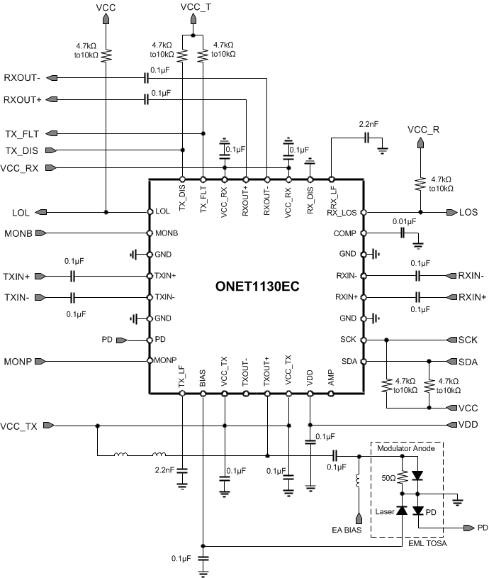
Simplified Schematic

4 Revision History
Changes from * Revision (June 2015) to A Revision
- Changed From: Product Preview To Production Go