SBOS427F June 2017 – March 2021 OPA145 , OPA2145
PRODUCTION DATA
- 1 Features
- 2 Applications
- 3 Description
- 4 Revision History
- 5 Pin Configuration and Functions
- 6 Specifications
- 7 Detailed Description
- 8 Application and Implementation
- 9 Power Supply Recommendations
- 10Layout
- 11Device and Documentation Support
- 12Mechanical, Packaging, and Orderable Information
Package Options
Mechanical Data (Package|Pins)
Thermal pad, mechanical data (Package|Pins)
Orderable Information
3 Description
The OPA145 and OPA2145 (OPAx145) devices are part of a family of low-power JFET input amplifier that have excellent drift, low current noise, and pico-ampere input bias current. These features make the OPAx145 an excellent choice for amplifying small signals from high-impedance sensors.
The rail-to-rail output swing interfaces to modern, single-supply, precision, analog-to-digital converters (ADCs) and digital-to-analog converters (DACs). In addition, the input range that includes V– allows designers to simplify power management and take advantage of the single-supply, low-noise JFET architecture.
| PART NUMBER | PACKAGE | BODY SIZE (NOM) |
|---|---|---|
| OPA145 | SOIC (8) | 4.90 mm × 3.91 mm |
| VSSOP (8) | 3.00 mm × 3.00 mm | |
| SOT-23 (5) | 2.90 mm × 1.60 mm | |
| OPA2145 | SOIC (8) | 4.90 mm × 3.91 mm |
| VSSOP (8) | 3.00 mm × 3.00 mm |
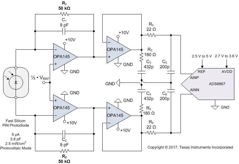
 OPAx145 Excels in 16-bit,
100-kSPS Fully Differential Transimpedance Imaging Application
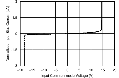
 OPAx145 Precision JFET
Technology Offers Excellent Linear Input Impedance