SBOS477B December 2011 – December 2016 OPA1652 , OPA1654
PRODUCTION DATA.
- 1 Features
- 2 Applications
- 3 Description
- 4 Revision History
- 5 Pin Configuration and Functions
- 6 Specifications
- 7 Detailed Description
- 8 Application and Implementation
- 9 Power Supply Recommendations
- 10Layout
- 11Device and Documentation Support
- 12Mechanical, Packaging, and Orderable Information
Package Options
Mechanical Data (Package|Pins)
Thermal pad, mechanical data (Package|Pins)
- DRG|8
Orderable Information
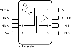
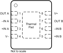
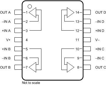
5 Pin Configuration and Functions
OPA1652 D and DGK Packages
8-Pin SOIC and VSSOP
Top View

OPA1652 DRG Package
8-Pin WSON With Exposed Thermal Pad
Top View

Pin Functions: OPA1652
| PIN | I/O | DESCRIPTION | |
|---|---|---|---|
| NAME | NO. | ||
| –IN A | 2 | I | Inverting input, channel A |
| +IN A | 3 | I | Noninverting input, channel A |
| –IN B | 6 | I | Inverting input, channel B |
| +IN B | 5 | I | Noninverting input, channel B |
| OUT A | 1 | O | Output, channel A |
| OUT B | 7 | O | Output, channel B |
| V– | 4 | — | Negative (lowest) power supply |
| V+ | 8 | — | Positive (highest) power supply |
| Thermal pad | — | — | Exposed thermal die pad on underside of DRG package; connect thermal die pad to V–. Soldering the thermal pad improves heat dissipation and provides specified performance |
OPA1654 D and PW Packages
14-Pin SOIC and TSSOP
Top View

Pin Functions: OPA1654
| PIN | I/O | DESCRIPTION | |
|---|---|---|---|
| NAME | NO. | ||
| –IN A | 2 | I | Inverting input, channel A |
| +IN A | 3 | I | Noninverting input, channel A |
| –IN B | 6 | I | Inverting input, channel B |
| +IN B | 5 | I | Noninverting input, channel B |
| –IN C | 9 | I | Inverting input, channel C |
| +IN D | 10 | I | Noninverting input, channel C |
| –IN D | 13 | I | Inverting input, channel D |
| +IN D | 12 | I | Noninverting input, channel D |
| OUT A | 1 | O | Output, channel A |
| OUT B | 7 | O | Output, channel B |
| OUT C | 8 | O | Output, channel C |
| OUT D | 14 | O | Output, channel D |
| V– | 11 | — | Negative (lowest) power supply |
| V+ | 4 | — | Positive (highest) power supply |