SBOS861A June   2017  – June 2018 OPA180-Q1 , OPA2180-Q1

PRODUCTION DATA.  

  1. Features
  2. Applications
  3. Description
    1.     Low Noise (Peak-to-Peak Noise = 250 nV)
  4. Revision History
  5. Device Comparison Table
  6. Pin Configuration and Functions
    1.     Pin Functions: OPA180-Q1
    2.     Pin Functions: OPA2180-Q1
  7. Specifications
    1. 7.1 Absolute Maximum Ratings
    2. 7.2 ESD Ratings
    3. 7.3 Recommended Operating Conditions
    4. 7.4 Thermal Information: OPA180-Q1
    5. 7.5 Thermal Information: OPA2180-Q1
    6. 7.6 Electrical Characteristics: VS = ±2 V to ±18 V (VS = 4 V to 36 V)
    7. 7.7 Typical Characteristics: Table of Graphs
    8. 7.8 Typical Characteristics
  8. Detailed Description
    1. 8.1 Overview
    2. 8.2 Functional Block Diagram
    3. 8.3 Feature Description
      1. 8.3.1 Operating Characteristics
      2. 8.3.2 EMI Rejection
      3. 8.3.3 Phase-Reversal Protection
      4. 8.3.4 Capacitive Load and Stability
      5. 8.3.5 Electrical Overstress
    4. 8.4 Device Functional Modes
  9. Application and Implementation
    1. 9.1 Application Information
    2. 9.2 Typical Applications
      1. 9.2.1 Bipolar ±10-V Analog Output from a Unipolar Voltage Output DAC
        1. 9.2.1.1 Design Requirements
        2. 9.2.1.2 Detailed Design Procedure
          1. 9.2.1.2.1 Component Selection
        3. 9.2.1.3 Application Curves
      2. 9.2.2 Discrete INA + Attenuation
      3. 9.2.3 RTD Amplifier
  10. 10Power Supply Recommendations
  11. 11Layout
    1. 11.1 Layout Guidelines
    2. 11.2 Layout Example
  12. 12Device and Documentation Support
    1. 12.1 Related Links
    2. 12.2 Trademarks
    3. 12.3 Electrostatic Discharge Caution
    4. 12.4 Glossary
  13. 13Mechanical, Packaging, and Orderable Information

Package Options

Mechanical Data (Package|Pins)
Thermal pad, mechanical data (Package|Pins)
Orderable Information

Capacitive Load and Stability

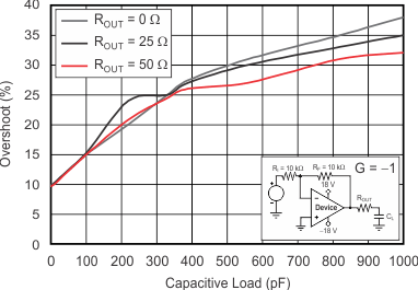
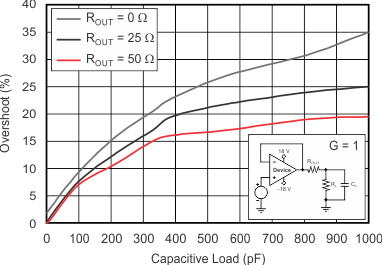
The dynamic characteristics of the OPAx180-Q1 are optimized for a range of common operating conditions. The combination of low closed-loop gain and high capacitive loads decreases the phase margin of the amplifier and can lead to gain peaking or oscillations. As a result, heavier capacitive loads must be isolated from the output. The simplest way to achieve this isolation is to add a small resistor (for example, ROUT equal to 50 Ω) in series with the output. Figure 27 and Figure 28 illustrate graphs of small-signal overshoot versus capacitive load for several values of ROUT. See the Feedback Plots Define Op Amp AC Performance, application report, available for download from the TI website, for details of analysis techniques and application circuits.
OPA180-Q1 OPA2180-Q1 tc_sm_oshoot-cl_pos_bos584.gif
RL = 10 kΩ 100-mV output step
Figure 27. Small-Signal Overshoot Versus Capacitive Load
OPA180-Q1 OPA2180-Q1 tc_sm_oshoot-cl_neg_bos584.gif
RL = 10 kΩ 100-mV output step
Figure 28. Small-Signal Overshoot Versus Capacitive Load